
What an 8-Layer PCB Manufacturer Must Prove Before Production
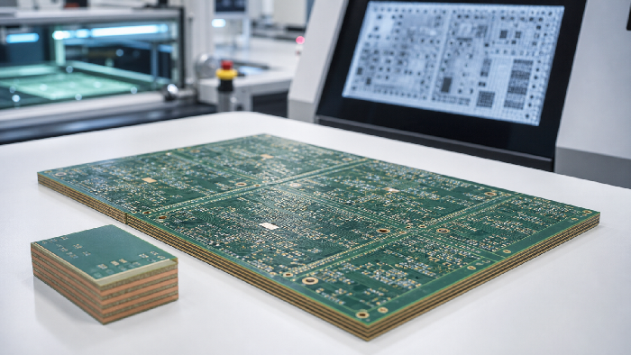
Table of Conent
Table of Conent
An 8-layer PCB manufacturer must prove more than layer-count capability. They should control stackup, registration, via quality, impedance, surface finish, inspection, and assembly handoff before your design enters production.
If your design team is still planning the layer structure, start with our 8-layer PCB guide. Supplier selection should come after the electrical and mechanical goals are clear.
Capability Questions to Ask First
Eight-layer PCBs are common, but not every supplier handles dense BGA routing, controlled impedance, or HDI features with the same process margin.
| Question | Why It Matters |
|---|---|
| Can you confirm a stackup before fabrication? | Prevents impedance and thickness surprises |
| What drill and via sizes are stable? | Protects plating reliability |
| Do you support via-in-pad or microvias? | Needed for some fine-pitch BGAs |
| Can you test controlled impedance? | Adds confidence for high-speed nets |
| What inspection is available after assembly? | Finds solder defects before shipment |
A strong supplier answers with process ranges and review steps, not vague promises.
Ask for Evidence, Not Just Capability Claims
Most manufacturers will say they can build 8-layer boards. The useful question is how they control the build. Ask for a sample stackup, a DFM review example, and the inspection methods they recommend for your component mix.
If your board has a fine-pitch BGA, ask whether they have built similar fanout structures. If your board has controlled impedance, ask how they confirm the stackup and whether test coupons are available. If your board will be assembled, ask how they inspect hidden joints.
The goal is not to interrogate the supplier. The goal is to learn whether their normal process fits your board.
Stackup Review Is Non-Negotiable
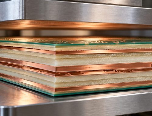
The 8-layer stackup decides trace impedance, return paths, plane coupling, and board thickness. If your manufacturer cannot provide a stackup drawing, do not release production.
Ask for:
- Layer order and function.
- Core and prepreg thickness.
- Copper weight per layer.
- Material grade.
- Finished thickness tolerance.
- Impedance geometry.
- Any HDI or sequential lamination notes.
For projects that include flexible or rigid-flex sections, compare requirements with our rigid-flex PCB guide.
Manufacturing Review Before Quote Approval
Before approving an 8-layer PCB manufacturer, ask them to review the design in three areas: fabrication, assembly, and test.
| Review Area | What Should Be Checked |
|---|---|
| Fabrication | Stackup, drill, annular ring, copper balance, finish |
| Assembly | BOM, placement, stencil, polarity, thermal pads |
| Test | Electrical test, AOI, X-ray, ICT or functional test |
Many sourcing problems happen because only the fabrication side is reviewed. A board can be easy to laminate and still be difficult to assemble. A dense connector area, poor test access, or a QFN thermal pad can create production trouble after bare-board approval.
HDI Needs a Different Conversation
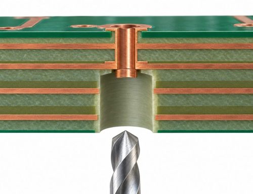
Some 8-layer designs can be built with standard through vias. Others need laser microvias or via-in-pad because the BGA pitch leaves no room for conventional fanout.
| Feature | Standard Multilayer | HDI-Oriented Build |
|---|---|---|
| Via type | Mechanical through vias | Blind, buried, or microvias |
| Lamination | Single lamination | Sequential lamination may be needed |
| Cost | Lower | Higher |
| Best fit | Moderate density | Fine-pitch BGA and compact products |
Do not add HDI because it sounds advanced. Add it when the component pitch and routing density require it.
HDI Questions for Supplier Qualification
If HDI may be required, ask:
- What microvia structure do you support?
- Do you recommend stacked or staggered microvias?
- Is via-in-pad filling and plating available?
- What reliability checks are used for microvias?
- How does HDI change lead time and cost?
The supplier should explain the trade-off clearly. If they push HDI without explaining why, be cautious. If they reject HDI without reviewing the BGA pitch, be cautious as well.
Surface Finish and Assembly Planning
For dense 8-layer boards, ENIG is often selected because it gives a flat solderable surface for fine-pitch packages. Other finishes can work, but the choice should match the component mix and storage plan.
Our guide to PCB surface treatment processes covers the trade-offs.
Also ask about component sourcing. Dense designs often use many small passives, fine-pitch ICs, and connectors with long lead-time risk. See what customers should note when purchasing components in SMT production.
Component Sourcing and Traceability
An 8-layer PCBA often contains expensive ICs and many small passives. The PCB manufacturer may also become the assembly and sourcing partner, so component control matters.
Ask how the supplier handles:
- Authorized distributor sourcing.
- Alternative part approval.
- Moisture-sensitive device storage.
- Lot traceability.
- Incoming inspection.
- Shortage communication.
| Risk | Supplier Control |
|---|---|
| Counterfeit or grey-market parts | Authorized sourcing and traceability |
| Wrong substitution | Written customer approval |
| Moisture damage | MSL handling and baking rules |
| Assembly delay | Early BOM review |
| Test failure | Incoming and post-assembly inspection |
Good sourcing reduces risk before the parts ever reach the SMT line.
Inspection Plan for an 8-Layer PCBA
The bare board can pass electrical test while the assembled board still has hidden solder defects. For 8-layer PCBAs, inspection should match package risk.
| Inspection Method | Best Use |
|---|---|
| AOI | Polarity, placement, visible solder joints |
| X-ray | BGA, QFN, hidden pads |
| ICT | Net-level and component-level checks |
| Functional test | Product behavior under real conditions |
For more detail, read our PCBA testing guide.
Communication Quality Matters
For 8-layer boards, communication is a manufacturing capability. You need clear answers on stackup, material, component availability, engineering questions, and inspection results.
Good communication looks like this:
- 1. The supplier asks questions before production, not after defects appear.
- 2. DFM issues include screenshots or exact locations.
- 3. Material or component substitutions require approval.
- 4. Lead time is separated by fabrication, sourcing, assembly, and testing.
- 5. Test failures are reported with evidence and proposed next steps.
If communication is vague before payment, it rarely becomes better during a production problem.
FAQ: Choosing an 8-Layer PCB Manufacturer
Is every 8-layer PCB manufacturer also an HDI manufacturer?
No. Standard 8-layer fabrication and HDI fabrication are different capability levels. If your board needs microvias or via-in-pad, verify that capability separately.
Should I send ODB++ instead of Gerbers?
ODB++ can reduce ambiguity because it carries more design intent, but many manufacturers can work from Gerbers. The key is to include complete drill, stackup, BOM, placement, and drawings when needed.
What inspection should I require?
At minimum, bare-board electrical test for fabrication and AOI for assembly. Add X-ray for BGA, QFN, LGA, or other hidden joints.
How do I compare two quotes?
Compare included stackup review, material, finish, controlled impedance, electrical test, assembly inspection, sourcing, packaging, and lead time. Do not compare unit price alone.
When should I involve the manufacturer?
Before routing is finalized. For dense 8-layer designs, stackup and via decisions should be reviewed early.
Quote Comparison Checklist
Use a structured comparison when reviewing 8-layer PCB manufacturer quotes. Do not choose only by unit price.
| Quote Area | What to Compare |
|---|---|
| Stackup | Is the construction documented and approved? |
| Material | Is the laminate named or generic? |
| Finish | Is ENIG, OSP, or HASL specified clearly? |
| Impedance | Is calculation or coupon testing included? |
| HDI | Are microvias, via filling, and lamination steps included? |
| Assembly | Does the quote include stencil, setup, AOI, and X-ray? |
| Components | Are parts sourced from approved channels? |
| Test | Is functional or ICT coverage included? |
If a quote is missing these details, it is not ready for a serious comparison. Ask the supplier to clarify before making a sourcing decision.
Production Handoff Requirements
For production builds, ask the manufacturer to keep a controlled record of the stackup, material, finish, test method, and approved substitutions. This matters when you reorder months later.
A common issue is silent change. The first batch uses one material, the second batch uses another equivalent material, and the product still works in basic testing. Later, EMC or temperature margin changes. The root cause is hard to trace because the construction change was not documented.
Good manufacturers control that risk with job records, approval steps, and traceability.
Final Recommendation
Choose the supplier that makes risk visible. An 8-layer PCB manufacturer should not only promise capability. They should explain stackup options, ask about impedance, review BGA fanout, recommend inspection, and document assumptions. That is the difference between a vendor and a manufacturing partner.
Engineering Handoff Checklist
Before you release an 8-layer PCB to a manufacturer, prepare a short handoff checklist. It should include the approved stackup, target impedance values, critical component notes, finish requirement, assembly inspection needs, and any test fixture constraints.
This checklist helps prevent a common problem: the electrical engineer, PCB designer, buyer, and manufacturer each assume someone else already explained the critical details. Dense boards do not tolerate that kind of gap.
| Handoff Item | Owner |
|---|---|
| Stackup and impedance | PCB designer and manufacturer |
| BOM substitutions | Engineering and procurement |
| Assembly notes | Manufacturing engineer |
| Test coverage | Test engineer and supplier |
| Packaging requirements | Quality or operations team |
Clear ownership keeps the order moving and reduces last-minute questions.
Red Flags
Avoid suppliers that quote without asking about stackup, impedance, BGA pitch, material, or assembly. Be cautious if they cannot explain how they inspect hidden solder joints or how they handle component substitutions.
A common example: an IoT gateway with a fine-pitch processor is ordered as a standard 8-layer board. The supplier accepts the Gerbers, but the via strategy leaves marginal annular rings. The first batch works inconsistently after thermal cycling. The issue began before fabrication, during supplier review.
Final Checklist
Before selecting an 8-layer PCB manufacturer, confirm:
- 1. Stackup is documented.
- 2. Via strategy is manufacturable.
- 3. Impedance requirements are reviewed.
- 4. Surface finish matches assembly.
- 5. Electrical test is included.
- 6. AOI and X-ray are available when needed.
- 7. Component sourcing is controlled.
AssyPCB provides 8-layer PCB fabrication, DFM review, component sourcing, assembly, AOI, X-ray, ICT, and functional testing. Send your files early and we will identify risk before it becomes rework.
Latest Blog

Contact Info
Phone: +86-755-82882936
Email: [email protected]
WhatsApp: +86-13570802455
Wechat: +86-13570802455
Address: 2nd floor,D Bldg.,Electric Link Technology Bldg.,Gongming,Guangming New Dist.,518106 Shenzhen, China