
10-Layer PCB Stackup Planning for Complex Electronics
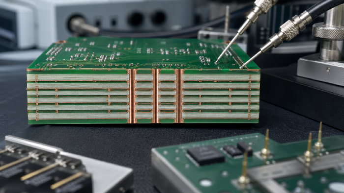
Table of Conent
Table of Conent
A 10-layer PCB is used when routing density, signal integrity, power distribution, and shielding need more room than 8 layers can provide. It is a practical layer count for complex embedded systems, communication equipment, industrial controls, and dense processor boards.
The extra layers only help if they are assigned clearly. A 10-layer PCB with poor reference-plane planning can perform worse than a disciplined 8-layer design.
When a 10-Layer PCB Is Justified
Use 10 layers when the design needs more than routing convenience. The reasons should be electrical, mechanical, or production-related.
| Driver | Why 10 Layers Help |
|---|---|
| High pin-count processor | More BGA escape and routing channels |
| Several high-speed interfaces | More reference-plane and impedance options |
| Multiple power rails | Cleaner power planes and decoupling |
| EMI-sensitive product | Better shielding and loop control |
| Compact board outline | More routing density without increasing size |
For high-frequency requirements, compare material and stackup needs with our RF PCB guide.
When 8 Layers Are Not Enough
Many designs sit in the gray zone between 8 and 10 layers. The board may route on 8 layers, but only with compromises: high-speed pairs jump layers too often, power rails crowd signal channels, or BGA breakout consumes too much space.
Ten layers give the layout team more room to keep reference planes clean. They also help preserve test points and reduce via congestion. That matters in production because a board that barely routes is often harder to inspect, debug, and revise.
The decision should be based on risk. If 10 layers prevent an EMC failure, high-speed margin problem, or painful BGA escape, the added bare-board cost may be justified.
Example 10-Layer Stackup
A common 10-layer stackup balances outer routing, internal routing, and reference planes.
| Layer | Function | Notes |
|---|---|---|
| L1 | Signal and components | Short critical routes |
| L2 | Ground | Reference for L1 |
| L3 | Signal | Internal controlled routing |
| L4 | Power | Main power distribution |
| L5 | Ground | Plane shielding |
| L6 | Ground or power | Depends on PDN needs |
| L7 | Signal | Internal routing |
| L8 | Power or ground | Supports rail planning |
| L9 | Ground | Reference for L10 |
| L10 | Signal and components | Secondary routing |
The right stackup depends on target impedance, board thickness, copper weight, and materials. Confirm it with the fabricator before final routing.
Alternative Stackup Goals
Different 10-layer boards need different priorities.
| Priority | Stackup Direction |
|---|---|
| High-speed digital | More signal layers adjacent to ground |
| Power integrity | Closely coupled power and ground planes |
| EMI control | Multiple solid ground planes |
| Dense BGA escape | Internal routing layers with clear references |
| Mixed-signal precision | Physical and return-path separation |
The stackup should not be copied from a random example without checking trace widths, impedance, and board thickness. Use examples as starting points, then validate with the manufacturer.
Via Planning Becomes Critical
As layer count increases, via decisions affect routing density, signal quality, and manufacturing yield. Through vias are simple and reliable, but they consume routing area on every layer. Blind, buried, or microvias can improve density but add cost and process complexity.
| Via Choice | Best Fit | Trade-Off |
|---|---|---|
| Through via | Robust general routing | Uses space on all layers |
| Blind via | BGA escape and HDI routing | Requires additional process control |
| Buried via | Internal routing density | Adds lamination complexity |
| Via-in-pad | Fine-pitch packages | Needs filling and plating control |
For basic drill constraints, see standard PCB hole drill sizes.
Via Stub and High-Speed Behavior
Through vias create unused barrel sections when a signal only travels between certain layers. At moderate speeds, this may not matter. At higher speeds, via stubs can create signal integrity problems.
Options include careful layer assignment, backdrilling, blind vias, or routing high-speed nets on layers that reduce transition length. The best choice depends on frequency, edge rate, cost target, and manufacturer capability.
Do not add advanced via processes blindly. Ask whether the signal actually needs them and whether the supplier can build them reliably.
Signal Integrity and Power Integrity
In a 10-layer PCB, signal integrity is not only about trace width. It is about reference continuity, return current, via transitions, plane spacing, and decoupling.
Good practice includes:
- Keep high-speed signals close to continuous ground.
- Avoid routing critical nets across plane splits.
- Use ground stitching near signal layer changes.
- Keep differential pairs consistent through breakouts.
- Place decoupling capacitors close to power pins.
- Review via stubs for very fast channels.
If the board has several rails and fast edges, involve the manufacturer before design release. Small stackup changes can affect impedance and power-plane behavior.
Thermal and Mechanical Planning
Many 10-layer boards carry processors, power devices, radio modules, or dense regulators. Thermal design should be reviewed with the mechanical and assembly plan.
| Thermal Concern | PCB-Level Design Response |
|---|---|
| Hot regulator | Thermal vias, copper spreading, airflow path |
| Processor heat | Plane spreading and heat sink interface |
| Dense power rail | Wider copper and via arrays |
| Enclosed product | Material and temperature review |
| Warpage risk | Balanced copper and symmetric stackup |
Thicker multilayer boards can store and spread heat, but they can also trap heat if copper and enclosure paths are not planned. Thermal vias must connect to useful copper, not just exist under a pad.
Manufacturing and Test Risks
Ten layers increase lamination and registration demands. A qualified manufacturer should check DFM, copper balance, drill tolerance, annular ring, and electrical testing before build.
| Risk | Prevention |
|---|---|
| Registration shift | Stable lamination and adequate annular rings |
| Warpage | Balanced copper and symmetric construction |
| Impedance mismatch | Confirmed stackup and coupon strategy |
| Hidden assembly defects | AOI, X-ray, ICT, or functional test |
| Field failure | Controlled sourcing and traceability |
Complex PCBAs need stronger testing. Our article on manufacturing test challenges for complex PCBAs explains why.
Design Review Checklist Before Release
Before sending a 10-layer PCB to production, review:
- 1. Stackup approved by manufacturer.
- 2. Controlled impedance table included.
- 3. Reference planes uninterrupted under critical nets.
- 4. Via strategy reviewed for density and signal speed.
- 5. Power rails assigned clearly.
- 6. Thermal vias and copper areas verified.
- 7. Drill aspect ratios within capability.
- 8. Surface finish matched to package types.
- 9. Test points preserved.
- 10. Assembly inspection requirements documented.
Skipping this review often creates problems that appear much later, during bring-up or certification testing.
Cost Control Without Cutting the Wrong Corners
The best way to reduce 10-layer PCB cost is to keep the design inside a stable process window. Do not force minimum trace, spacing, drill, and via-in-pad everywhere unless the design requires it.
You can often control cost by:
- 1. Using standard material where performance allows.
- 2. Avoiding unnecessary HDI.
- 3. Keeping copper balanced.
- 4. Confirming stackup early.
- 5. Designing for panel utilization.
- 6. Planning test access before layout is locked.
For the full production flow, see multilayer PCB design to production.
Frequently Asked Questions About 10-Layer PCBs
Is a 10-layer PCB considered advanced?
It is advanced compared with simple 2-layer or 4-layer boards, but it is routine for qualified multilayer manufacturers. The difficulty depends on density, material, vias, impedance, and assembly complexity.
Does a 10-layer PCB require HDI?
Not always. Many 10-layer boards use through vias. HDI is considered when BGA pitch, board size, or signal performance requires it.
Can a 10-layer board use standard FR-4?
Yes, if the electrical, thermal, and reliability requirements allow it. Use high-Tg or low-loss materials when the design requires better temperature or frequency performance.
What is the biggest cost driver?
Layer count matters, but HDI features, fine lines, tight drill limits, material selection, impedance testing, surface finish, and assembly inspection can be just as important.
When should I involve the fabricator?
Before final routing. Stackup, impedance, and via decisions should be confirmed early.
Example: 10-Layer PCB for a Communication Gateway
A communication gateway may include an application processor, memory, Ethernet switching, wireless module, isolated power, and several external connectors. The first layout attempt may fit on 8 layers, but it often creates routing compromises around the processor and high-speed interfaces.
Moving to 10 layers allows cleaner BGA escape, better ground reference, and more controlled power distribution. It can also preserve production test access, which becomes difficult when every layer is crowded.
The value shows up during validation. Cleaner return paths reduce noise. Better power distribution improves stability. More test access makes failures easier to isolate. These are engineering advantages, not just layout convenience.
Manufacturing Notes for 10-Layer Release
Before release, ask the fabricator to confirm:
- Whether the stackup is symmetric.
- Whether dielectric spacing matches impedance needs.
- Whether through vias meet aspect ratio limits.
- Whether any HDI process is required.
- Whether copper balance is acceptable.
- Whether the surface finish matches assembly.
- Whether the test plan matches the product risk.
If the board has fast serial channels, RF sections, or dense BGA routing, schedule this review before design freeze.
Final Engineering Advice
A 10-layer PCB should make the design more controlled, not just more complex. Use the layers to protect reference planes, simplify routing, organize power, and make test access possible. If the extra layers do not improve those areas, revisit whether 8 layers would be enough.
Documentation to Keep With the Design
Keep the manufacturing decisions with the design files. Future revisions become much easier when the next engineer can see why the stackup, material, via structure, and finish were chosen.
Useful documentation includes:
- Approved stackup drawing.
- Impedance table.
- Material and surface finish.
- Via design rules.
- Controlled nets list.
- Assembly inspection plan.
- Known DFM exceptions.
- Test access notes.
This documentation is especially valuable when the design moves from prototype to production or when a second supplier is evaluated. Without it, the team may repeat old decisions without understanding the original trade-offs.
Bottom Line
A 10-layer PCB is a powerful tool for complex electronics, but it rewards planning. Define the stackup, protect reference planes, choose vias deliberately, and involve the manufacturer before the layout becomes fixed.
AssyPCB can review your 10-layer stackup, check manufacturability, fabricate the bare boards, source components, assemble the PCBAs, and run the right inspection plan before shipment.
Latest Blog
Contact Info
Phone: +86-755-82882936
Email: [email protected]
WhatsApp: +86-13570802455
Wechat: +86-13570802455
Address: 2nd floor,D Bldg.,Electric Link Technology Bldg.,Gongming,Guangming New Dist.,518106 Shenzhen, China