
Selecting a 10-Layer PCB Manufacturer Without Creating Production Risk
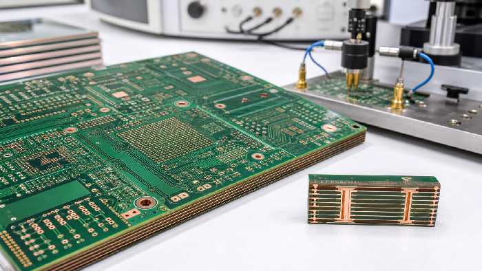
Table of Conent
Table of Conent
A 10-layer PCB manufacturer should act like an engineering partner, not only a board shop. At this layer count, stackup control, via strategy, impedance review, lamination quality, component sourcing, and testing all affect whether the final product works reliably.
For design-side planning, start with our 10-layer PCB stackup guide. This article focuses on manufacturer evaluation.
The Manufacturer Must Review the Stackup
Do not send a 10-layer design to production without a stackup confirmation. The stackup affects impedance, thickness, power integrity, via aspect ratio, and assembly flatness.
Ask for:
- Material type and Tg.
- Core and prepreg construction.
- Copper weight per layer.
- Finished thickness tolerance.
- Impedance geometry.
- Via and drill capability.
- Controlled impedance test method, if required.
| Supplier Behavior | Risk Level |
|---|---|
| Provides stackup before quote finalization | Low |
| Provides stackup only after order | Medium |
| Will not document stackup | High |
What Stackup Review Should Include
A good stackup review is not just a layer list. It should connect the physical build to the electrical goals.
| Stackup Item | Why It Matters |
|---|---|
| Dielectric spacing | Determines impedance geometry |
| Copper thickness | Affects etching, current, and impedance |
| Plane order | Controls return paths and shielding |
| Material Tg | Supports assembly temperature and reliability |
| Finished thickness | Affects connectors and enclosure fit |
| Symmetry | Helps reduce bow and twist |
If your manufacturer cannot explain these relationships, they may be quoting the board without really reviewing the design.
HDI and Via Capability
Many 10-layer boards can use standard through vias. Others need blind vias, buried vias, or via-in-pad because of BGA density. The manufacturer should help decide, not simply accept every feature in the files.
| Feature | Manufacturing Impact |
|---|---|
| Mechanical through vias | Lower cost, robust, more routing blockage |
| Blind vias | Better escape routing, added process steps |
| Buried vias | More internal density, more lamination complexity |
| Filled via-in-pad | Fine-pitch BGA support, higher process control |
If the supplier cannot explain the cost and yield impact of these choices, they may not be the right fit for a 10-layer PCB.
High-Speed and Impedance Support
At 10 layers, high-speed requirements are common. The manufacturer should support impedance review before fabrication and should be comfortable discussing trace geometry.
Ask for:
- Standard impedance stackup options.
- Trace width and spacing recommendations.
- Coupon testing availability.
- Tolerance expectations.
- Guidance for differential pairs.
- Notes on via transitions and backdrilling, if relevant.
| Signal Group | Supplier Input Needed |
|---|---|
| PCIe or similar fast serial links | Stackup, via strategy, impedance |
| Ethernet | Differential pair geometry |
| RF sections | Material, finish, and loss review |
| DDR or memory buses | Routing consistency and reference planes |
| Clocks | Return path and isolation |
The supplier does not replace signal integrity simulation, but they do control the physical stackup that makes the simulation meaningful.
File Package and Communication
A complete data package shortens review and prevents assumptions. For a 10-layer PCBA, include fabrication and assembly files together.
Send Gerbers or ODB++, drill files, stackup notes, impedance table, board drawing, BOM, placement file, assembly drawing, test instructions, and any controlled components list.
Our guide to documents required by PCB assembly gives a useful checklist.
Communication During Engineering Questions
Engineering questions are normal on a 10-layer board. The issue is how they are handled.
Good communication includes exact location references, screenshots, recommended fixes, and clear impact on lead time or cost. Poor communication uses vague warnings like “too small” or “please check” without showing the problem.
If a supplier asks no questions at all, that is not automatically good. It may mean the board is simple, or it may mean nobody reviewed it carefully.
Component Sourcing Is Part of the Risk
Dense 10-layer boards often include processors, memory, RF parts, power modules, and many small passives. A manufacturer that also sources components should control substitutions, traceability, moisture-sensitive devices, and packaging.
Ask:
- 1. Are parts sourced from authorized distributors?
- 2. How are substitutions approved?
- 3. How are moisture-sensitive components stored?
- 4. Can the supplier flag lifecycle or shortage risks?
- 5. Is traceability available for production builds?
For more, see component purchasing notes for SMT production.
Assembly Planning for Dense 10-Layer PCBAs
A 10-layer bare board is only part of the product. Dense assemblies need stencil design, placement review, reflow planning, and inspection.
| Assembly Issue | Why It Matters |
|---|---|
| BGA package | Hidden solder joints need X-ray |
| QFN thermal pad | Stencil aperture affects voiding |
| Fine-pitch connector | Solder bridging risk |
| Tall components | Fixture and test access |
| Moisture-sensitive ICs | Storage and baking control |
Ask whether the same team reviews fabrication and assembly data. If not, the board may be manufacturable but still difficult to assemble at stable yield.
Inspection and Test Requirements
A 10-layer PCB manufacturer should support more than visual inspection. The assembled board may need AOI, X-ray, ICT, boundary-scan support, or functional test.
| Test Method | Use It When |
|---|---|
| Electrical test | Every bare board production run |
| AOI | SMT assembly with visible joints |
| X-ray | BGA, QFN, LGA, hidden pads |
| ICT | Production boards with accessible test points |
| Functional test | Product behavior must be verified before shipment |
Read our PCBA testing process guide before defining the inspection plan.
Test Access Should Be Designed In
Production testing becomes much harder if test points are removed late in layout. Dense 10-layer boards often lose test access because every square millimeter feels valuable.
Before release, ask:
- Which rails need test pads?
- Which programming interface needs access?
- Which communication ports need functional checks?
- Can the fixture reach bottom-side pads?
- Are tall parts blocking probes?
- Is boundary scan available for dense digital devices?
Testing is not a separate manufacturing step. It is a design requirement.
Cost Evaluation
The lowest 10-layer PCB quote can be misleading. Review what is included: stackup engineering, controlled impedance, electrical test, finish, packaging, assembly inspection, and lead time.
Our guide to PCB price composition explains how these factors shape the real cost.
FAQ: Selecting a 10-Layer PCB Manufacturer
Can any multilayer PCB supplier build 10 layers?
Many can build 10 layers, but not all can support dense routing, controlled impedance, HDI features, assembly, and testing with the same reliability.
Should the manufacturer help choose the stackup?
Yes. The design team defines electrical intent, but the manufacturer should confirm materials, dielectric spacing, copper, and build feasibility.
Is via-in-pad always expensive?
It adds process steps because vias may need filling and plating. Use it where package density requires it, not as a default design habit.
What should I check before approving a quote?
Confirm stackup, material, finish, electrical test, impedance support, assembly inspection, component sourcing, packaging, and lead time.
Why choose a one-stop PCB and PCBA supplier?
One supplier can review fabrication, assembly, sourcing, and test together. That reduces handoff gaps between board fabrication and finished product delivery.
Supplier Scorecard
Use this scorecard when comparing suppliers for a 10-layer PCB.
| Category | Strong Supplier Signal |
|---|---|
| Stackup | Provides documented construction before production |
| Engineering | Gives specific DFM and DFA feedback |
| Impedance | Reviews trace geometry against real materials |
| Via process | Explains through, blind, buried, and via-in-pad trade-offs |
| Assembly | Reviews BOM, placement, stencil, and inspection |
| Sourcing | Uses approved channels and controls substitutions |
| Testing | Supports AOI, X-ray, ICT, and functional test |
| Communication | Gives clear answers with evidence |
If a supplier is weak in one category, decide whether that weakness matters for your product. For a simple prototype, limited testing may be acceptable. For a production gateway, medical device, industrial controller, or aerospace assembly, it may not be.
Risk Questions Before Purchase Order
Before issuing a purchase order, ask:
- 1. What assumptions are included in the quote?
- 2. What design changes would reduce cost or improve yield?
- 3. Which items could extend lead time?
- 4. Which components have sourcing risk?
- 5. Which inspection steps are included?
- 6. What will be verified before shipment?
The answers often reveal whether the manufacturer is thinking ahead. A strong supplier helps you avoid problems before they enter the factory.
Final Recommendation
For 10-layer boards, choose the manufacturer with the best engineering process, not only the lowest price. The board is complex enough that stackup, assembly, sourcing, and test decisions can change the success of the whole product.
What to Expect From a Good First Review
A good manufacturer review should not take weeks, but it should produce useful comments. For a 10-layer PCB, expect questions about stackup, impedance, drill sizes, via structure, BGA fanout, surface finish, assembly inspection, and test access.
The review may identify cost-saving changes too. For example, the manufacturer may suggest a slightly larger via, a more standard dielectric spacing, a different panel arrangement, or a finish that better matches the component package. These recommendations can improve yield without changing the product function.
| Review Output | Why It Helps |
|---|---|
| Stackup confirmation | Locks electrical assumptions |
| DFM issues list | Prevents fabrication defects |
| DFA comments | Reduces assembly risk |
| Sourcing notes | Prevents BOM delays |
| Test suggestions | Improves production coverage |
If the first review contains no meaningful feedback, ask whether the supplier truly reviewed the files or only priced them.
Long-Term Supplier Fit
The best 10-layer PCB manufacturer for one prototype may not be the best supplier for long-term production. For repeat builds, prioritize process stability, documentation, traceability, and communication.
Ask whether they can keep the same approved stackup for repeat orders, notify you before material substitutions, support revision control, and provide inspection records. Those details matter when the product has a service life measured in years.
Final Supplier Checklist
Choose a 10-layer PCB manufacturer that can:
- Confirm stackup before production.
- Review controlled impedance.
- Explain via and HDI options.
- Provide DFM and DFA feedback.
- Source components with traceability.
- Inspect hidden solder joints.
- Run electrical and functional tests.
AssyPCB supports 10-layer PCB fabrication, engineering review, authorized component sourcing, SMT assembly, AOI, X-ray, ICT, and functional testing. Send your files early and we will help reduce risk before the first panel is built.
Latest Blog

Contact Info
Phone: +86-755-82882936
Email: [email protected]
WhatsApp: +86-13570802455
Wechat: +86-13570802455
Address: 2nd floor,D Bldg.,Electric Link Technology Bldg.,Gongming,Guangming New Dist.,518106 Shenzhen, China