
12-Layer PCB Design Guide for High-Density Hardware
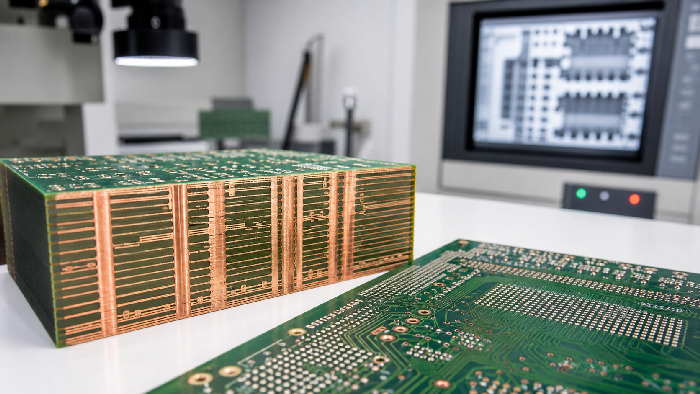
Table of Conent
Table of Conent
A 12-layer PCB is used when a design needs high routing density, several reference planes, multiple power domains, and tighter control of signal integrity than lower layer counts can provide. It is common in advanced industrial, communication, medical, aerospace, and embedded computing products.
At 12 layers, the board is no longer just “more routing space.” It is a controlled electromechanical structure. Stackup, material, via type, plane order, and test strategy all need to be planned together.
When 12 Layers Are the Right Choice
Choose 12 layers when a lower layer count creates unacceptable compromises.
| Design Requirement | Why 12 Layers Help |
|---|---|
| High pin-count BGA | More escape routing and layer assignment options |
| Several high-speed interfaces | More continuous reference planes |
| Multiple power rails | Cleaner PDN and decoupling paths |
| Tight EMI requirements | Better shielding and return-current control |
| Compact product size | Density without increasing outline |
| Reliability-critical assembly | More room for test points and routing discipline |
For general context, see multilayer PCB design to production.
The Real Reason to Add Layers
The right reason to choose a 12-layer PCB is not “more layers are better.” The right reason is that the board needs controlled routing, reference planes, power distribution, and manufacturing margin at the same time.
For example, a compact medical controller may include a processor, memory, isolated power, sensor inputs, wireless communication, and safety-related connectors. An 8-layer board might route, but the layout may sacrifice test points, ground continuity, or power-plane organization. A 12-layer PCB gives the design enough structure to protect the important circuits.
That structure has value only when it is planned. If the extra layers become random routing space, the board can still be noisy, hard to build, and difficult to test.
Example 12-Layer Stackup Thinking
The exact stackup depends on the design, but a useful 12-layer structure usually alternates signal and reference layers so fast nets are never far from ground.
| Layer Group | Typical Purpose |
|---|---|
| L1-L2 | Components, short signals, ground reference |
| L3-L4 | Internal signal and power distribution |
| L5-L6 | Ground and high-speed routing reference |
| L7-L8 | Power and ground or signal/reference pair |
| L9-L10 | Internal signal and reference plane |
| L11-L12 | Ground reference and bottom-side routing |
The important point is not the exact order in this table. The important point is that every critical signal layer needs a clean return path.
Stackup Priorities for 12 Layers
| Priority | Design Implication |
|---|---|
| High-speed signals | Route near continuous ground |
| Power integrity | Use plane pairs and short decoupling paths |
| EMI control | Preserve shielding and reduce loop area |
| BGA escape | Reserve layers for clean fanout |
| Thermal paths | Connect heat sources to useful copper |
| Manufacturing yield | Keep vias, copper, and lamination balanced |
At 12 layers, the stackup should be reviewed with the fabricator before routing is complete. Waiting until release can force difficult geometry changes.
HDI Decisions
Some 12-layer PCBs use standard through vias. Others need blind vias, buried vias, microvias, or via-in-pad. HDI can improve BGA escape routing and reduce via stubs, but it adds cost and process control requirements.
| Option | Benefit | Cost or Risk |
|---|---|---|
| Through vias | Robust and economical | Consumes routing space on all layers |
| Blind vias | Better outer-layer escape | Additional process steps |
| Buried vias | Frees outer layers | More lamination complexity |
| Microvias | Supports fine-pitch density | Requires strict process control |
| Filled via-in-pad | Useful for BGA pads | Adds filling and plating requirements |
Do not specify HDI features until the package pitch and routing strategy justify them.
HDI Reliability Questions
If HDI is required, reliability depends on both design and process control. Ask the manufacturer about microvia structure, lamination sequence, via filling, inspection, and design rules.
| HDI Question | Why It Matters |
|---|---|
| Stacked or staggered microvias? | Affects reliability and cost |
| Via-in-pad filled and capped? | Needed for solderable BGA pads |
| Sequential lamination count? | Affects lead time and yield |
| Microvia diameter and capture pad? | Determines manufacturability |
| Test and inspection method? | Confirms process control |
HDI is powerful, but it is not free design space. Use it where it solves a real density or signal problem.
Signal Integrity, RF, and Power Integrity
A 12-layer PCB often carries sensitive and fast circuits. The stackup must support impedance, return paths, and power stability.
Use these rules:
- Route critical nets over continuous ground.
- Keep high-speed layer transitions short and well-stitched.
- Avoid plane splits under fast signals.
- Keep power and ground close where decoupling matters.
- Separate noisy switching loops from sensitive analog paths.
- Review material choice for RF or high-frequency sections.
If RF behavior is important, compare material choices with our RF and high-frequency PCB guide.
Power Distribution Network Planning
A 12-layer PCB may have many voltage rails. The power distribution network should be planned before routing density takes over the board.
Key questions:
- Which rails carry high transient current?
- Which rails feed sensitive analog circuits?
- Which rails need tight noise control?
- Where will decoupling capacitors connect?
- Are power and ground planes close enough for low inductance?
- Are split planes creating return-path problems?
| PDN Problem | Design Response |
|---|---|
| Processor current spikes | Local decoupling and low-inductance plane paths |
| Analog noise | Separate routing and clean references |
| Switching regulator noise | Compact hot loops and controlled placement |
| Multiple rails | Clear plane islands and return planning |
| Thermal stress | Copper spreading and via arrays |
Power integrity and signal integrity are connected. A noisy rail can create timing, RF, and measurement problems that look unrelated at first.
Manufacturing Risks at 12 Layers
The main risks are registration, lamination stability, warpage, via reliability, and inspection coverage. These are manageable, but not accidental.
| Risk | Practical Control |
|---|---|
| Layer misregistration | Adequate annular ring and stable lamination |
| Warpage | Symmetric stackup and copper balance |
| Via failure | Proper aspect ratio and plating control |
| Impedance drift | Confirmed material and dielectric spacing |
| Assembly defects | AOI, X-ray, ICT, and functional testing |
For board flatness issues, read methods to prevent PCB deformation.
Material, Finish, and Reliability Choices
Material choice becomes more important as layer count rises. Standard FR-4 may be acceptable for many 12-layer boards, but high temperature, high frequency, or regulated applications may need stronger material control.
| Requirement | Material or Process Consideration |
|---|---|
| Lead-free assembly | Tg and thermal robustness |
| High-frequency section | Low-loss laminate or hybrid stackup |
| Medical or aerospace use | Traceability and documentation |
| Fine-pitch assembly | ENIG or another flat finish |
| High current | Copper weight and thermal design |
| Long service life | Reliability testing and controlled sourcing |
Surface finish should be chosen for assembly and reliability, not appearance. Dense 12-layer boards often use ENIG because it supports fine-pitch soldering and storage better than rougher finishes.
Test Planning Before Layout Lock
Testing should not be added after routing is complete. Complex 12-layer PCBAs need test access planned early.
At minimum, discuss bare-board electrical test, AOI, X-ray for hidden joints, in-circuit test, and functional test. If your board has firmware-controlled interfaces, include boot and programming steps in the test plan.
Our article on manufacturing test challenges for complex PCBAs explains why dense assemblies need stronger validation. For inspection methods, see the PCBA testing process guide.
Production Test Coverage
For a 12-layer PCBA, test coverage should match product risk. Bare-board electrical testing is not enough once expensive components are mounted.
| Test Method | Typical Role |
|---|---|
| Bare-board electrical test | Finds fabrication opens and shorts |
| AOI | Checks placement and visible solder joints |
| X-ray | Checks BGA, QFN, and hidden solder joints |
| ICT | Verifies nets and components where access exists |
| Functional test | Confirms real product behavior |
| Programming test | Confirms firmware loading and boot behavior |
Design test access early. It is much easier to keep a few probe pads during layout than to add them after the board is already dense.
DFM and DFA Checklist
Before releasing a 12-layer PCB, review both fabrication and assembly.
- 1. Stackup approved by fabricator.
- 2. Material and Tg confirmed.
- 3. Controlled impedance table included.
- 4. HDI structures reviewed, if used.
- 5. Via aspect ratios within capability.
- 6. Copper balance checked.
- 7. Reference planes protected.
- 8. Power rails and returns reviewed.
- 9. Surface finish matched to assembly.
- 10. Test access preserved.
- 11. AOI and X-ray requirements documented.
- 12. Component sourcing and substitutions controlled.
This level of review may feel slow, but it is faster than diagnosing unstable boards after assembly.
Frequently Asked Questions About 12-Layer PCBs
Is a 12-layer PCB overkill for most products?
Yes, for simple products. It is justified when density, signal integrity, power distribution, EMI, or reliability requirements cannot be handled cleanly with fewer layers.
Does 12 layers mean the board must use HDI?
No. Some 12-layer boards use standard through vias. HDI is used when fine-pitch packages, routing density, or signal performance require it.
Can a 12-layer PCB be built at 1.6 mm thickness?
Sometimes, but it depends on copper weight, dielectric spacing, impedance, and manufacturing capability. The stackup should be confirmed before routing.
What is the biggest risk in 12-layer PCB design?
The biggest risk is treating the stackup as an afterthought. Reference planes, via transitions, power integrity, and manufacturing limits must be planned together.
When should I contact the manufacturer?
Before final placement and routing. For 12-layer designs, early manufacturer input can prevent expensive stackup and via changes later.
Example: 12-Layer PCB for a High-Reliability Control Unit
Picture a high-reliability control unit with a processor, memory, isolated communication, analog measurement, power conversion, and safety-critical connectors. The board must fit a fixed enclosure and pass environmental testing.
On fewer layers, the design may route, but return paths become harder to protect. Power rails compete with signal channels. Test points disappear. Sensitive analog traces run closer to noisy switching paths.
A 12-layer PCB gives the design team enough structure to separate functions without making the board larger. The extra layers support cleaner planes, more deliberate routing, and better test access. The result is not automatically reliable, but it gives the engineering team the right tools.
Supplier Review Points
Before ordering a 12-layer PCB, ask the manufacturer to review the design for:
- Stackup symmetry.
- Controlled impedance.
- Via structure and aspect ratio.
- HDI reliability, if used.
- Copper balance.
- Material availability.
- Surface finish.
- Panelization.
- Assembly inspection.
- Functional test plan.
At this layer count, the supplier should be comfortable giving technical feedback. If they treat the job like a simple commodity board, the risk is too high.
Final Engineering Advice
Use 12 layers when the product needs structure, density, and reliability at the same time. Keep the stackup intentional, document the requirements, involve the manufacturer early, and design test access before layout space disappears. A good 12-layer PCB is not only dense. It is controlled.
Bottom Line
A 12-layer PCB is justified when density, speed, power distribution, and reliability requirements need a more controlled stackup. The design should be reviewed with the manufacturer before release, especially if HDI, impedance control, or regulated-industry documentation is involved.
AssyPCB can review your 12-layer stackup, check DFM and DFA risk, fabricate the boards, source components, assemble the PCBAs, and verify them with the right inspection plan.
Latest Blog

Contact Info
Phone: +86-755-82882936
Email: [email protected]
WhatsApp: +86-13570802455
Wechat: +86-13570802455
Address: 2nd floor,D Bldg.,Electric Link Technology Bldg.,Gongming,Guangming New Dist.,518106 Shenzhen, China