
Transistor Schematic Symbols: How to Read NPN, PNP, and FET Symbols
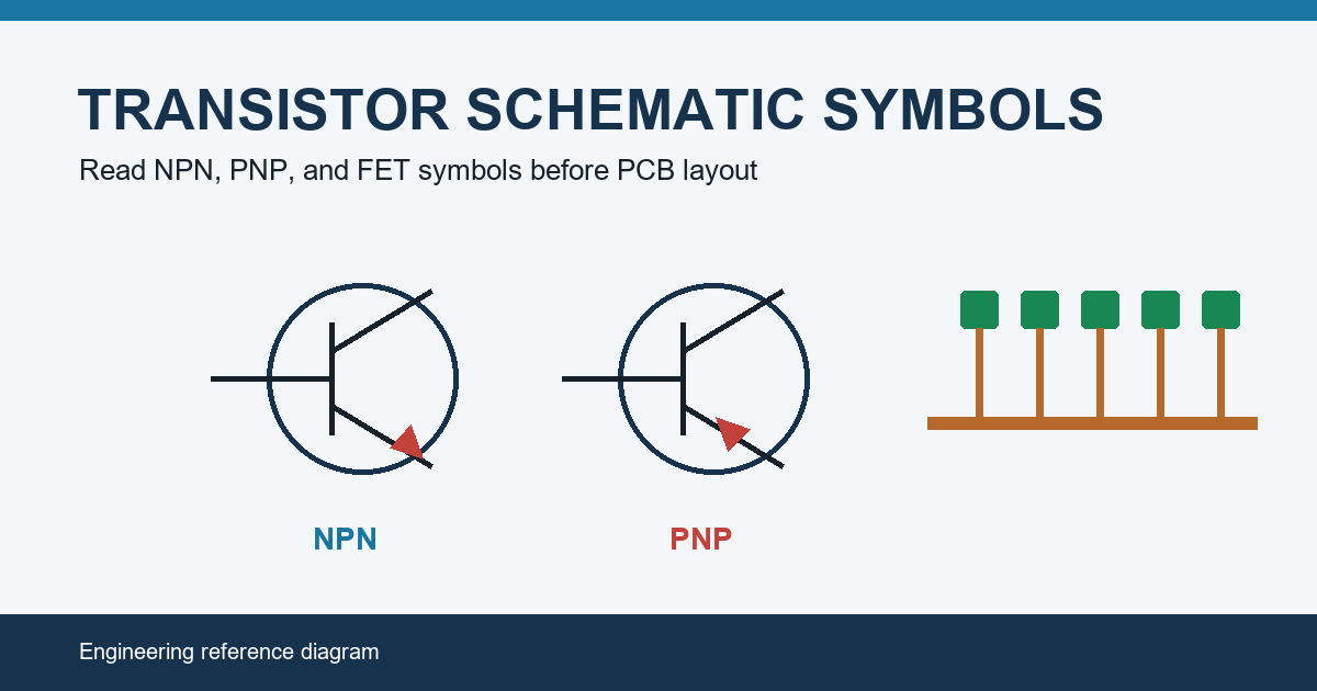
Table of Conent
Table of Conent
Transistor schematic symbols show what a device does electrically and how its terminals connect to the rest of a circuit. They do not show the physical package, lead order, or exact PCB footprint. That distinction matters: a schematic can be logically correct while the assembled board fails because the symbol pins were mapped to the wrong package pads.
This guide explains how to read the most common transistor symbols, distinguish NPN from PNP devices, identify FET and MOSFET terminals, and verify symbol-to-footprint mapping before PCB fabrication and assembly.
What a Transistor Symbol Represents
A transistor symbol is a functional abstraction. Lines, arrows, and terminal labels describe the device family and the intended direction of control or current flow. The symbol lets an engineer understand circuit behavior without drawing the semiconductor structure or package.
This is different from a PCB footprint. The footprint defines copper pads, drill holes, courtyard clearances, pin numbering, and component orientation on the physical board. It is also different from the package drawing in a datasheet, which may show the device from the top, bottom, or side.
If you need a refresher on resistors, capacitors, diodes, transistors, and other common parts, see the basic electronic components guide.
How to Read an NPN Transistor Symbol
The standard bipolar junction transistor, or BJT, has three terminals:
- Base (B): the control terminal.
- Collector (C): one side of the main current path.
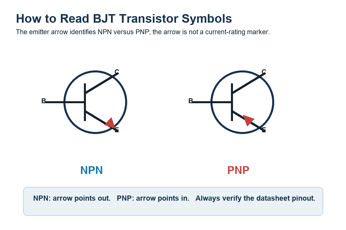
- Emitter (E): the terminal that carries the arrow in the schematic symbol.
On an NPN symbol, the emitter arrow points away from the base. A common memory aid is “NPN: Not Pointing iN.” The phrase is useful for recognition, but circuit analysis still requires the actual voltage polarities and current directions.
In a typical low-side switching circuit, the emitter connects toward ground, the load sits between the supply and collector, and base drive turns the device on. The base resistor, expected collector current, transistor gain assumptions, saturation voltage, and power dissipation must all be checked. The symbol alone does not establish those values.
How to Read a PNP Transistor Symbol
A PNP BJT uses the same base, collector, and emitter terminal names, but the emitter arrow points toward the base. PNP devices often appear in high-side switching circuits, current mirrors, complementary amplifier stages, and polarity-control functions.
The arrow tells you the transistor type; it does not tell you which physical lead is pin 1. Two PNP transistors in the same package style can have different lead assignments. For example, a three-lead package may use E-B-C, C-B-E, or another order depending on the part.
Before layout, compare the schematic library symbol against the manufacturer datasheet and the approved bill of materials. Never infer the lead order from package appearance or from another transistor with a similar part number.
BJT Symbol Variations You May Encounter
Not every BJT appears as the simple three-terminal symbol. Common variations include:
Darlington Transistors
A Darlington device combines two BJTs to provide high current gain. Its symbol usually shows two connected transistor stages inside one device. Darlington transistors generally have a higher effective base-emitter voltage and a higher saturation voltage than a single BJT, which affects drive calculations and thermal performance.
Phototransistors
A phototransistor symbol adds arrows pointing toward the transistor to indicate incoming light. Designers should distinguish those light arrows from the emitter arrow that differentiates NPN and PNP devices.
Digital or Pre-Biased Transistors
Some symbols include internal bias resistors. These parts can reduce external component count, but their fixed resistor values constrain the usable drive conditions. The exact internal network must match the selected manufacturer part.
Transistor Arrays
An array symbol may place several matched transistors in one package and may show shared terminals or a common substrate connection. Verify every unit and hidden power or substrate pin before approving the schematic.
FET and MOSFET Schematic Symbols
Field-effect transistors use different terminal names:
- Gate (G): the electric-field control terminal.
- Drain (D): one end of the controlled current path.
- Source (S): the other end of the controlled current path.
- Body or bulk (B): sometimes shown separately, but often internally tied to the source in discrete MOSFETs.
MOSFET symbols vary between standards and library conventions. Some show an explicit body diode, some show the body terminal, and others use a simplified three-terminal representation. Enhancement-mode and depletion-mode devices may use different channel-line styles. N-channel and P-channel devices use different arrow conventions, but the exact drawing style can differ among CAD libraries.
For that reason, do not identify a MOSFET only by arrow direction. Read the library description, manufacturer part number, terminal names, and datasheet together. The presence and orientation of the body diode is especially important in switching converters, motor drives, reverse-polarity protection, and hot-swap circuits.
Other Transistor Symbols
JFET symbols use gate, drain, and source terminals but show a junction gate rather than the insulated gate used by a MOSFET. IGBT symbols combine MOS-gate control with a bipolar conduction structure and usually label gate, collector, and emitter. Specialized devices such as unijunction transistors and phototransistors have their own symbols and should not be substituted with a generic BJT symbol.
When a schematic symbol is unfamiliar, the correct response is not to guess. Open the component library metadata and manufacturer datasheet, then verify the device family, terminal names, electrical ratings, package, and pin numbering.
Symbol Orientation Does Not Define Circuit Polarity
CAD tools allow symbols to be rotated and mirrored. A collector drawn at the bottom of the page is still the collector if the pin name says C. Likewise, a horizontally mirrored PNP symbol remains a PNP device.
Read terminal labels and net names instead of relying on page position. This becomes important in dense schematics where functional blocks are arranged for signal flow rather than for conventional symbol orientation.
From Schematic Symbol to PCB Footprint
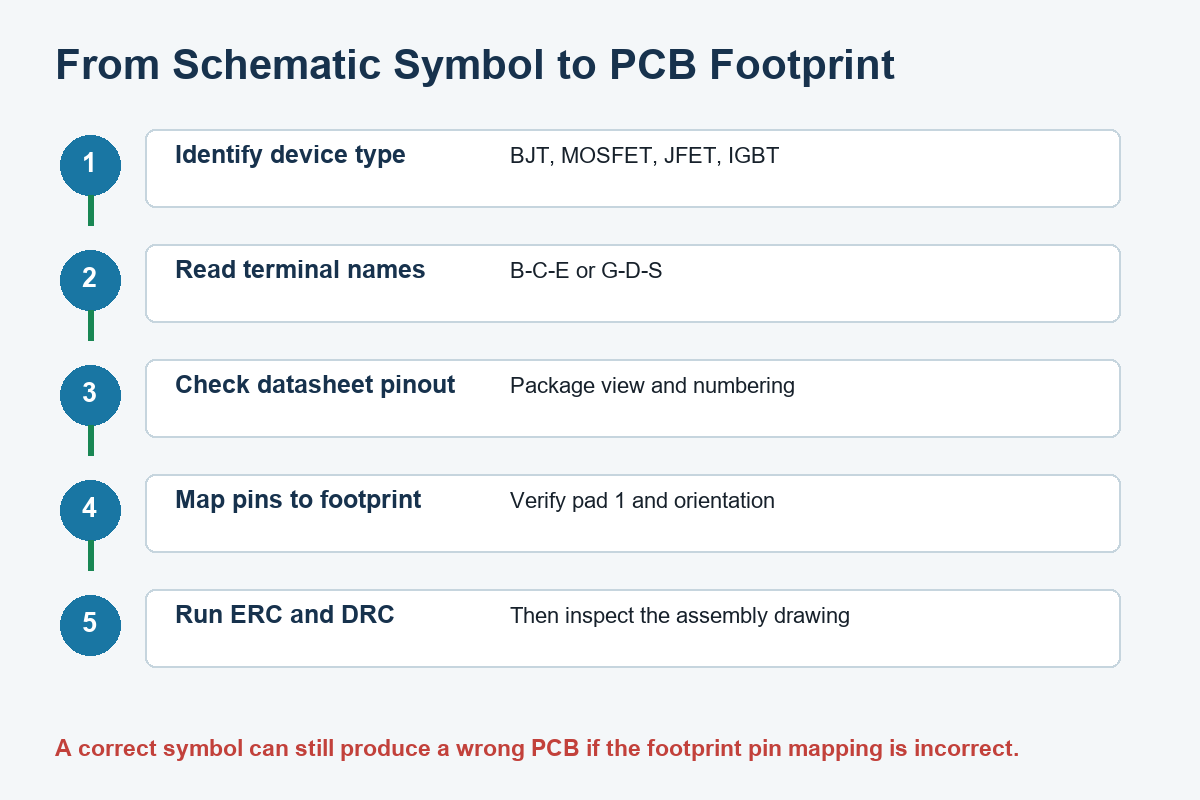
The highest-risk step is mapping logical symbol pins to physical footprint pads. A disciplined check follows this sequence:
- Confirm the exact manufacturer part number and acceptable alternates.
- Identify the device family and terminal names in the datasheet.
- Confirm whether the package drawing uses a top view or bottom view.
- Match each symbol pin number to the corresponding footprint pad number.
- Verify pin 1, polarity, thermal-pad numbering, and component orientation.
- Run electrical rule checking and design rule checking.
- Inspect the assembly drawing, pick-and-place rotation, and first-article documentation.
The PCB layout design guide provides additional context on turning a completed schematic into manufacturable board data.
Preparing a board for assembly? Submit the schematic, Gerber or ODB++ files, BOM, pick-and-place data, and assembly drawings through the PCB assembly service page so the package and orientation requirements can be reviewed with the build documentation.
Common Symbol and Footprint Mistakes
Swapping Collector and Emitter
A BJT may conduct weakly when collector and emitter are reversed, which can make a prototype appear intermittently functional. Gain, breakdown behavior, leakage, and saturation performance will not match the intended design.
Confusing NPN and PNP
Using the wrong polarity changes the required bias conditions. This mistake often comes from choosing a generic library symbol without checking the approved part number.
Assuming Every TO-92 Pinout Is the Same
TO-92 packages are commonly available with different lead orders. A familiar outline is not sufficient evidence for footprint mapping.
Mirroring an SMD Package
A datasheet may show the package from below while the CAD footprint is viewed from above. Misreading the view can mirror every connection.
Ignoring the MOSFET Body Diode
The intrinsic diode can create an unintended current path. Its orientation must be considered during schematic review and power-off analysis.
Omitting Thermal Pads or Exposed Connections
Power transistor packages may include an exposed pad that is electrically connected to the drain, collector, or another node. The schematic, footprint, copper area, vias, solder-paste aperture, and assembly instructions must treat it correctly.
Review Checklist Before Releasing PCB Files
Use this checklist during schematic and layout review:
- The symbol matches the device family and polarity.
- Terminal names match the manufacturer datasheet.
- Symbol pin numbers match footprint pad numbers.
- The datasheet viewing direction has been confirmed.
- Package suffixes in the BOM match the footprint.
- Alternate parts use compatible pinouts and electrical ratings.
- MOSFET body-diode direction is correct.
- Exposed pads and thermal connections are defined.
- Base or gate drive components support the required operating point.
- Voltage, current, power, switching, and thermal limits have margin.
- Assembly polarity and orientation indicators are visible.
- ERC and DRC results have been reviewed rather than waived without explanation.
For products moving from prototype to production, the custom PCB assembly page outlines an appropriate manufacturing path for builds that require controlled component placement and documented assembly requirements.
Final Takeaway
A transistor electronic symbol identifies the device family and logical terminals, but it does not guarantee a correct physical implementation. Read the emitter arrow to distinguish NPN and PNP BJTs, use terminal labels to interpret FET and MOSFET symbols, and verify every symbol pin against the exact datasheet and footprint.
Before releasing a build, prepare the schematic, fabrication data, BOM, pick-and-place file, assembly drawing, and any approved alternates. Send those files through the contact page for an engineering and quotation review of the PCB assembly package.
Latest Blog



Contact Info
Phone: +86-755-82882936
Email: [email protected]
WhatsApp: +86-13570802455
Wechat: +86-13570802455
Address: 2nd floor,D Bldg.,Electric Link Technology Bldg.,Gongming,Guangming New Dist.,518106 Shenzhen, China