
Full-Wave Rectifier vs Half-Wave Rectifier: Key Differences for PCB Design
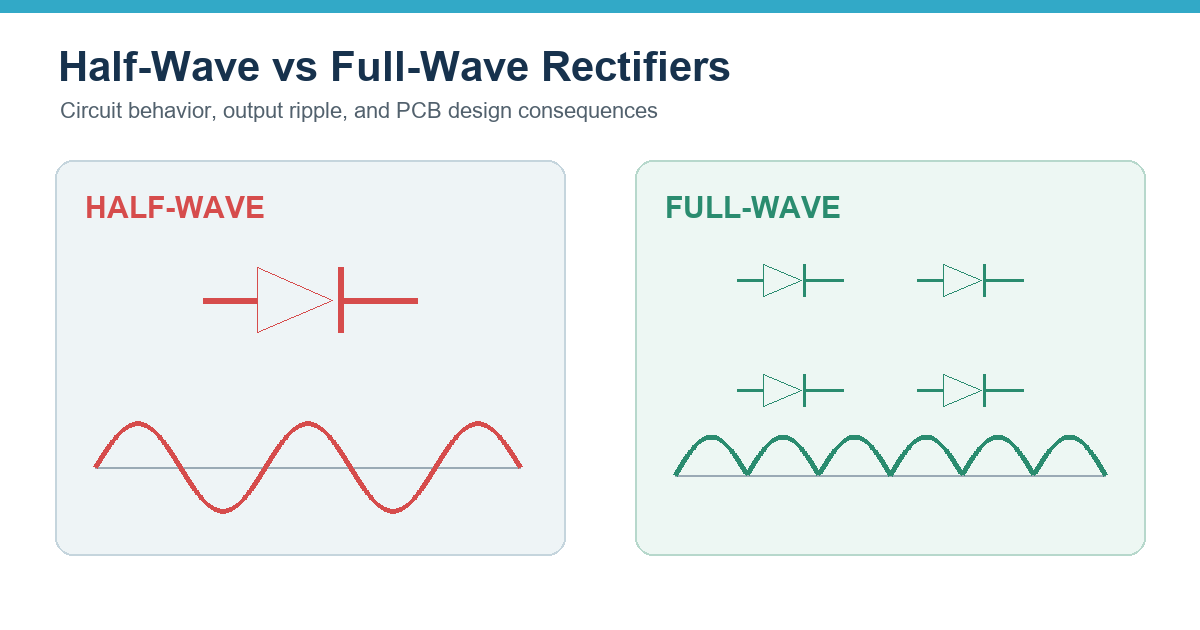
Table of Conent
Table of Conent
A half-wave rectifier uses only one half of an AC waveform, while a full-wave rectifier uses both halves. That basic difference changes the ripple frequency, average DC output, transformer utilization, diode count, heat distribution, filter-capacitor requirements, and the current paths that a PCB designer must control.
For most line-frequency power supplies that need useful DC power, a full-wave topology is the practical starting point. A half-wave circuit can still be appropriate when current is low, cost and component count dominate, and ripple or transformer DC bias will not create a reliability problem. The correct choice depends on the load, input source, safety architecture, thermal limits, and acceptable output ripple.
What Does a Rectifier Do?
A rectifier directs alternating current so that current through the load flows in one direction. The result is pulsating DC, not automatically a regulated DC rail. A practical supply may add a reservoir capacitor, an inductor, a regulator, protection components, and filtering after the rectifier.
The diode is the essential switching element in the simplest circuits. Its forward-voltage drop, reverse-voltage rating, recovery behavior, surge-current capability, leakage, package, and thermal path all affect the design. Readers who need a component-level refresher can review the basic PCB component functions before comparing the two topologies. Analog Devices also provides a concise definition of a half-wave rectifier.
Half-Wave Rectifier Operation
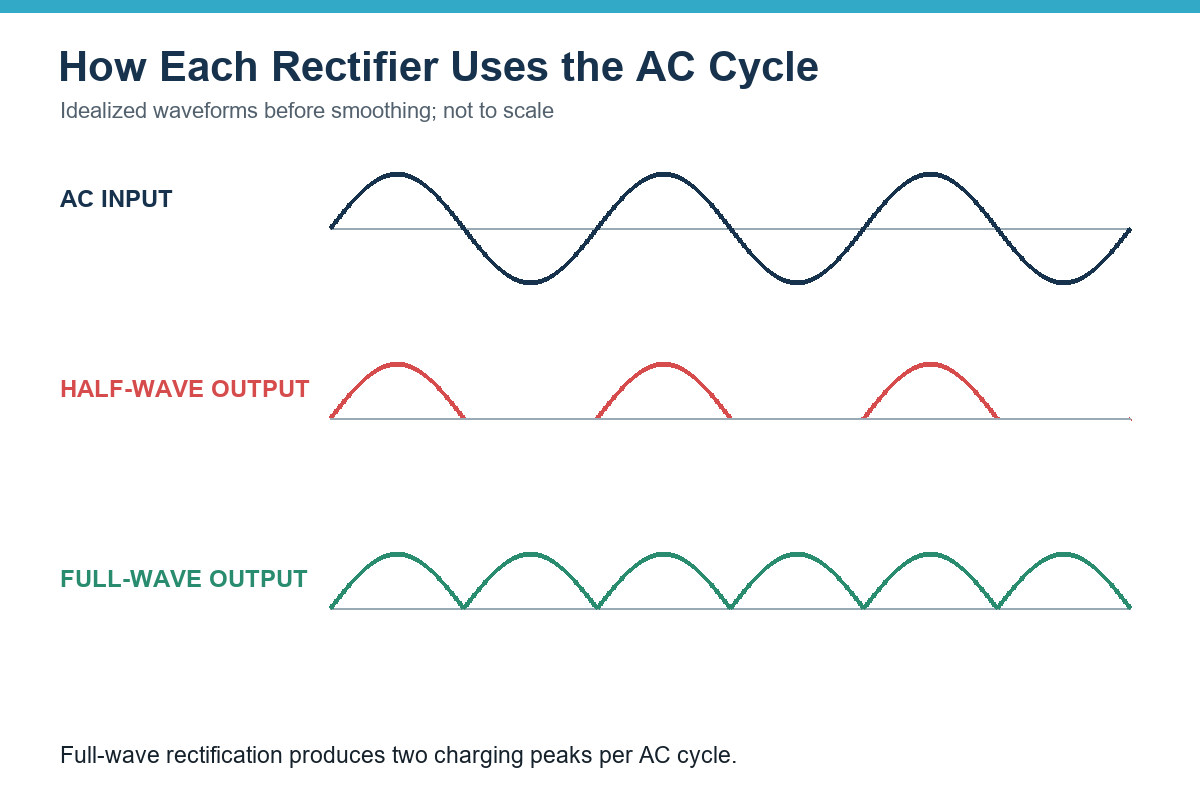
A basic half-wave rectifier places one diode in series with the load. During the forward-polarized half-cycle, the diode conducts. During the opposite half-cycle, it blocks. With a resistive load and ideal diode, the output contains one positive pulse for every complete AC cycle. If the line frequency is 60 Hz, the ripple repetition frequency is also 60 Hz.
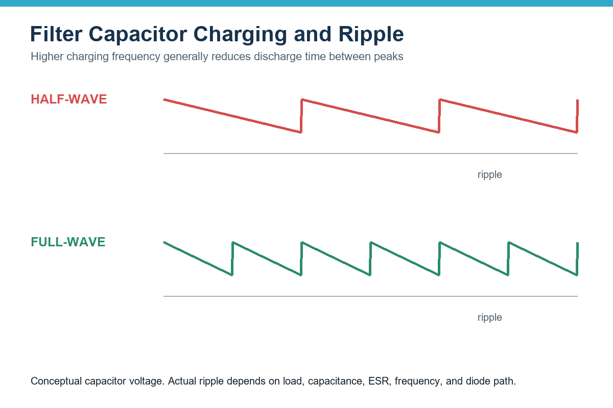
The main attraction is simplicity: one diode, a small footprint, and a straightforward current path. The penalty is that half of the source waveform does no useful work. The long interval between charging peaks forces a reservoir capacitor to support the load for more time. For the same load and allowed ripple, that usually means more capacitance than a full-wave design.
Half-wave current also has a DC component at the transformer secondary. Depending on the transformer and loading, that imbalance can increase heating, acoustic noise, or core saturation risk. This concern is easy to miss when a circuit that worked at a few milliamps is scaled to a higher load without revisiting the magnetic component.
Full-Wave Rectifier Operation
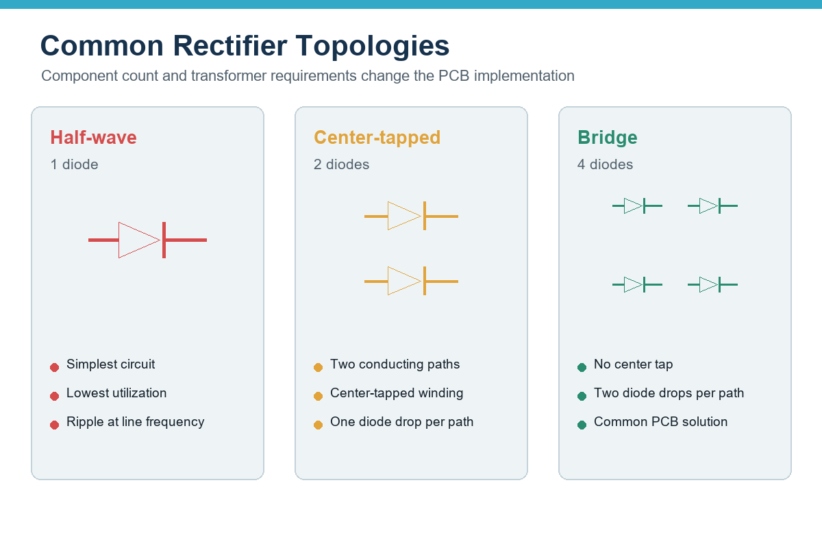
A full-wave rectifier redirects both halves of the AC cycle so current through the load keeps the same polarity. Designers commonly use either a center-tapped secondary with two diodes or a bridge with four diodes. In a bridge, two diodes conduct in series during each half-cycle. In a center-tapped circuit, one diode conducts at a time, but the transformer requires the appropriate winding.
Because both halves are used, a 60 Hz input produces 120 Hz ripple before regulation. The shorter time between charging peaks normally reduces ripple for the same load and capacitance. Full-wave rectification also makes better use of the transformer waveform and is generally preferred when power level, output quality, and transformer utilization matter.
The bridge is common because it does not require a center tap. However, its conducting path includes two diode drops. At low output voltages, those losses can consume a meaningful share of the power budget. A center-tapped topology has one diode drop in each active path, but each half of the secondary conducts on alternating half-cycles and each diode must tolerate the applicable reverse voltage.
Full-Wave vs Half-Wave Rectifier Comparison
| Design factor | Half-wave rectifier | Full-wave rectifier |
|---|---|---|
| AC waveform used | One half-cycle | Both half-cycles |
| Typical diode count | One | Two with a center tap or four in a bridge |
| Ripple frequency at 60 Hz input | 60 Hz | 120 Hz |
| Unfiltered average output | Lower for the same peak input | Higher for the same peak input |
| Filter requirement | More demanding for equal load and ripple | Less demanding because charging peaks occur more often |
| Transformer utilization | Lower; asymmetric loading can matter | Better waveform utilization |
| Conduction loss | One diode drop | One drop for center-tapped; two for bridge |
| Best fit | Very low-power, simple, noncritical loads | Most practical AC-to-DC power stages |
The familiar ideal values are useful for comparison, but they are not a production design guarantee. Real output depends on transformer regulation, diode drop, source impedance, capacitor ESR, load waveform, line tolerance, temperature, and downstream circuitry.
How the Choice Changes Filter Capacitor Sizing
A first-pass capacitor estimate for a rectifier followed by a reservoir capacitor is:
C approximately equals Iload divided by fripple times delta V.
Here, C is capacitance, Iload is load current, fripple is the charging-pulse frequency, and delta V is the allowed peak-to-peak ripple. At the same line frequency, load, and ripple target, doubling the ripple frequency roughly halves the ideal capacitance estimate. That is why a full-wave circuit can achieve a similar ripple target with less capacitance than a half-wave circuit.
This estimate is only a starting point. Verify capacitor voltage rating, capacitance tolerance, ESR, ripple-current rating, temperature life, inrush current, and load transients. The diode and transformer must also withstand narrow charging-current peaks that can be much higher than the average DC load current.
If you are preparing a prototype power board, send the input range, schematic, Gerber files, BOM, expected load, thermal limits, and test requirements through the prototype PCB assembly service for an engineering and build review.
Diode Ratings and Thermal Tradeoffs
Reverse-voltage margin
Each diode must survive the maximum reverse voltage created by the transformer, capacitor, line tolerance, and transient environment. Do not choose peak inverse voltage from nominal RMS input alone. Convert RMS voltage to peak, consider winding tolerances and no-load rise, then apply a margin appropriate to the application and protection strategy.
Forward loss and junction temperature
Estimate diode dissipation with the actual current waveform, not only the average load current. A bridge places two forward drops in the conducting path, while a basic half-wave or center-tapped path has one. Schottky diodes may reduce forward loss at suitable voltage levels, but leakage and reverse-voltage limits require attention. Fast-recovery or soft-recovery behavior may matter at higher switching frequencies.
Surge and repetitive peak current
At startup, an empty reservoir capacitor can behave like a short-duration heavy load. Check nonrepetitive surge rating, repetitive peak current, source impedance, fuse behavior, and the number of expected power cycles. The PCB pads and traces must carry this pulse without excessive heating or voltage drop.
PCB Layout Implications
The rectifier, transformer secondary or AC input connector, and first reservoir capacitor form a high-current charging loop. Keep this loop compact. Long traces increase resistance and loop area, which can worsen voltage drop, radiated noise, and ringing. Place the bulk capacitor close to the rectifier return and route sensitive analog or control grounds away from the pulsed charging current.
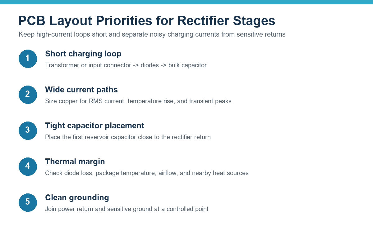
Size copper from RMS and peak current, acceptable temperature rise, copper weight, layer location, and airflow. Provide enough copper around power-diode pads for heat spreading when the package relies on PCB conduction. Keep required creepage and clearance around hazardous voltages; the correct spacing depends on working voltage, pollution degree, material group, coating, applicable standard, and product environment.
Assembly also affects reliability. Large electrolytic capacitors may need mechanical support, polarity controls, and adequate courtyard spacing. Diode orientation must be unambiguous in silkscreen and assembly documentation. The broader printed circuit board assembly process explains how design data becomes a finished PCBA, while this guide to PCB assembly quality control covers inspection and verification points that apply after placement and soldering.
When Should You Use Each Topology?
Choose a half-wave rectifier when:
- The load current is very low and intermittent.
- Ripple is acceptable or downstream filtering is sufficient.
- One-diode simplicity materially benefits cost or space.
- The source and transformer can tolerate asymmetric loading.
- Efficiency and transformer utilization are not primary constraints.
Choose a full-wave rectifier when:
- The circuit supplies meaningful continuous power.
- Lower ripple and smaller filtering components are valuable.
- Transformer utilization and output stability matter.
- The added diode count is acceptable.
- The design needs a conventional front end for regulation.
For PCB-based power conversion, a bridge rectifier is often the default full-wave choice because it works with a simple two-wire secondary. A center-tapped arrangement can be attractive when reducing the number of diode drops matters and the correct transformer is already available. Review the intended input, output, thermal, and assembly requirements against the relevant power supply PCB capability. OrinewPCB also publishes broader PCB manufacturing and assembly resources that can support related design-for-manufacturing research.
Files and Checks to Prepare Before PCB Assembly
Before releasing a rectifier board, verify the schematic against worst-case input voltage, minimum line, maximum load, startup, short-circuit behavior, and thermal conditions. Confirm diode polarity, capacitor polarity, transformer pinout, fuse placement, discharge paths, connector ratings, and test-point access.
A production package should include Gerber or ODB++ data, drill files, BOM with approved manufacturer part numbers, centroid or pick-and-place data, assembly drawings, polarity notes, fabrication requirements, and a test plan. Identify high-voltage nets and any safety-standard constraints. If substitutions are permitted, define electrical, package, lifecycle, and qualification boundaries rather than approving vague equivalents.
Final Selection
The central difference between a full-wave and half-wave rectifier is how much of the AC cycle reaches the load. From that difference follow the practical consequences: ripple frequency, capacitor size, transformer loading, diode loss, thermal behavior, and PCB current-loop design.
Use a half-wave circuit only when its simplicity outweighs its poorer waveform utilization and filtering burden. For most PCB power stages, evaluate a full-wave bridge or center-tapped design first, then select diodes, capacitance, copper, and spacing from worst-case electrical and thermal conditions.
For a manufacturing review and quotation, submit your Gerber files, BOM, pick-and-place data, required quantity, input and load conditions, applicable standards, and testing requirements through the PCB assembly quote page. The engineering review can then focus on manufacturability, sourcing, polarity control, thermal risk, and the inspection plan before the build begins.
Latest Blog



Contact Info
Phone: +86-755-82882936
Email: [email protected]
WhatsApp: +86-13570802455
Wechat: +86-13570802455
Address: 2nd floor,D Bldg.,Electric Link Technology Bldg.,Gongming,Guangming New Dist.,518106 Shenzhen, China