
LED Circuit Symbol: How to Read Polarity and PCB Connections
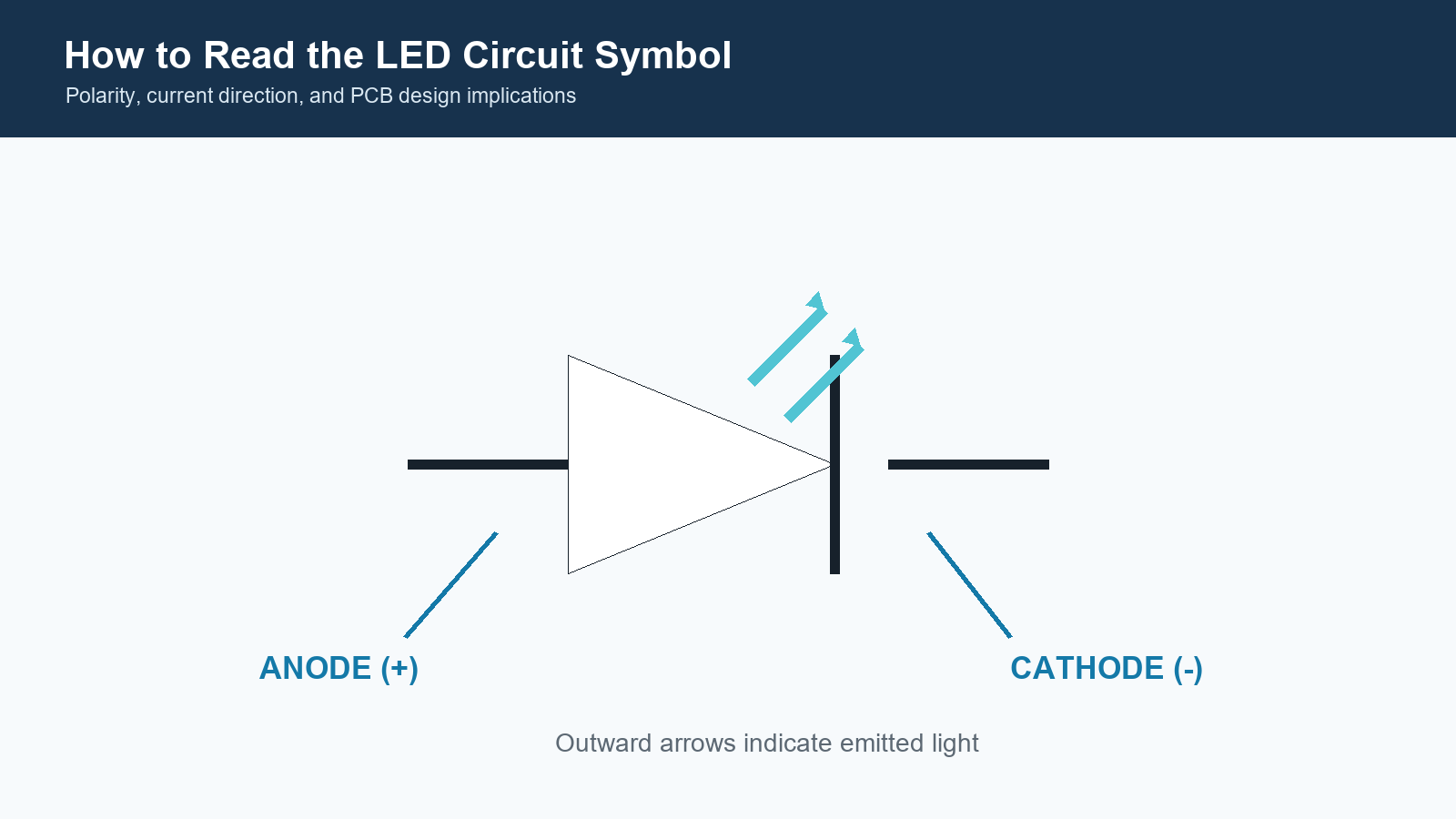
Table of Conent
Table of Conent
The LED circuit symbol identifies a light-emitting diode in a schematic. It uses the basic diode symbol plus two small arrows pointing away from the device. Those arrows represent emitted light. The symbol also shows polarity: the anode is the positive side under normal forward operation, and the cathode is the side marked by the vertical bar.
Reading the symbol correctly is only the first step. A working PCB also requires the right current-limiting method, supply headroom, footprint pin mapping, component orientation, and assembly documentation. A schematic can look correct while the assembled LED remains dark if any one of those details is wrong.
What the LED Circuit Symbol Means
An LED is a polarized semiconductor device. Under normal operation, conventional current enters the anode and leaves the cathode. When the forward voltage and current are within the component’s specified operating range, the LED emits light.
The schematic symbol communicates electrical function, not physical appearance. It does not tell you the package size, lens shape, color, brightness, viewing angle, maximum current, or exact pad numbering. Those details come from the approved manufacturer part number and datasheet.
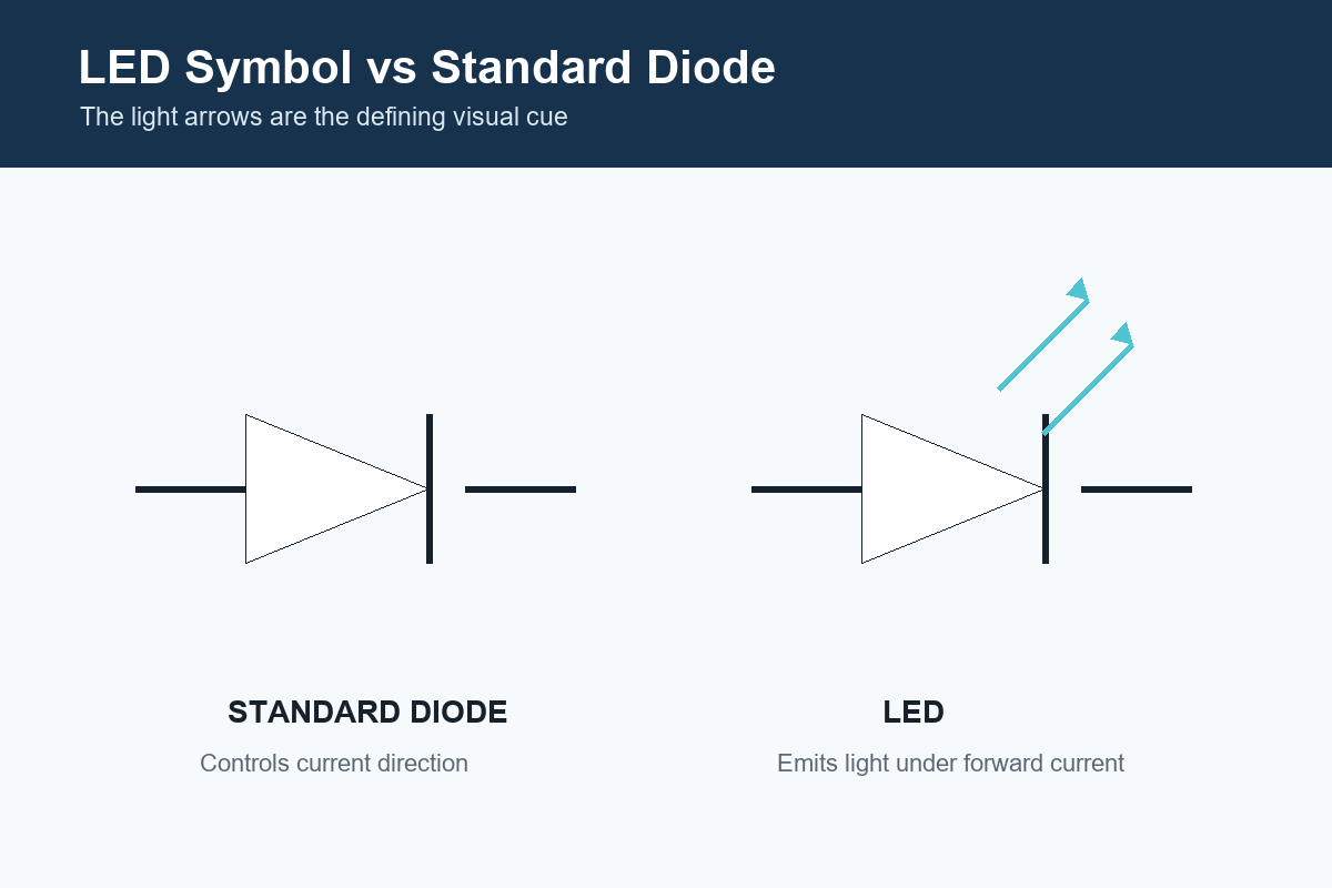
The two outward arrows are the quickest way to recognize the symbol. A photodiode uses a related drawing, but its arrows point toward the diode because light enters the device. If you are reviewing unfamiliar symbols across a larger circuit, the same separation between electrical symbol and physical package also applies in this transistor schematic symbol guide.
LED Symbol vs Standard Diode Symbol
A standard rectifier or switching diode and an LED share the same one-way current concept. Both have an anode and cathode, and both require the circuit designer to respect reverse-voltage and forward-current limits. The LED adds outward arrows to show that electrical energy is converted into light.
The symbol does not mean that every LED has the same forward voltage. Forward voltage varies with semiconductor chemistry, color, current, temperature, and part selection. A red indicator LED may need less forward voltage than a blue or white LED, but the design value must come from the selected component’s datasheet rather than a color-based assumption.
The symbol also does not replace circuit analysis. Rectifier diodes may carry much higher current or withstand much higher reverse voltage than a small indicator LED. The rectifier comparison guide shows how diode direction affects current paths in power-conversion circuits. For a broader explanation of LED construction and behavior, the SparkFun LED tutorial provides an accessible technical reference.
How to Identify Anode and Cathode
In the schematic, the vertical bar marks the cathode. The opposite terminal is the anode. During forward operation, the anode is at a higher electrical potential than the cathode.
Physical LEDs use several possible polarity indicators:
- A through-hole LED often has a longer anode lead and a shorter cathode lead.
- The package body may have a flat edge near the cathode.
- An SMD LED may use a notch, chamfer, colored mark, T-shaped mark, or underside pattern.
- A footprint may use a line, dot,
K,A, or pin-number marker.
These clues are useful, but none is universal. Leads may already be trimmed, package marks can vary by supplier, and CAD libraries may use different silkscreen conventions. Always verify the exact part’s datasheet and approved footprint. In documentation, A usually denotes the anode and K the cathode; K avoids confusion with C, which is used for other component terminals and reference designators.
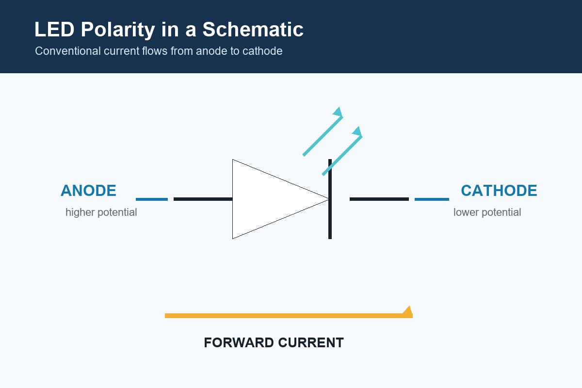
If an LED is installed backward, it normally blocks current and does not light. That does not mean reverse connection is harmless. Many LEDs have a relatively low allowable reverse voltage. A bipolar or reverse-prone circuit may need an antiparallel diode, bridge arrangement, or another protective design based on the actual operating conditions.
Reading an LED in a Complete Schematic
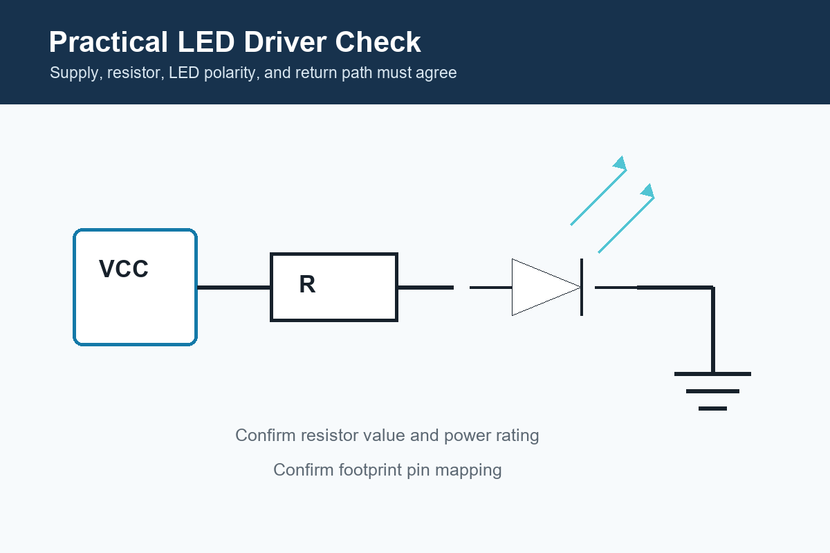
Do not review the LED symbol in isolation. Trace the complete current path from the supply, through the current-control element and LED, to the return node. Then check the control device and logic conditions that enable that path.
Supply voltage and return path
Identify the relevant supply rail and its tolerance. Confirm that the return symbol is the intended electrical reference, especially in circuits with isolated grounds, chassis ground, analog ground, or multiple power domains. Net labels can connect distant schematic locations without a visible wire, so review the net name and connectivity rather than only the page geometry.
Current-limiting resistor
Many indicator LEDs use a series resistor. For a simple DC example, the resistor can be estimated with:
R = (VSUPPLY - VF) / ILED
Example: with a 5.0 V supply, an assumed 2.0 V LED forward voltage, and a target current of 10 mA, the calculated resistance is 300 ohms. A designer would normally select an appropriate standard value and then verify current at supply and forward-voltage tolerances. The resistor’s power dissipation also needs margin:
P = ILED² x R
This example is not a universal LED recipe. Brightness requirements, pulsed drive, ambient temperature, component tolerance, optical efficiency, and the driver output voltage can change the correct operating point. High-power LEDs and strings often require constant-current drivers instead of a single resistor.
Driver transistor or IC
An LED may be driven directly from a logic output, by a BJT or MOSFET, through a constant-current sink, or from a dedicated LED driver. Check whether the control is active-high or active-low. A low-side transistor can make the LED turn on when its control node is asserted, while a high-side arrangement may reverse the apparent logic.
Also confirm the driver’s output current, voltage drop, startup state, PWM behavior, and thermal limits. Multiplexed displays require peak-current and duty-cycle analysis. LEDs connected to microcontroller pins must stay within both per-pin and total-port limits stated by the device manufacturer.
Preparing an LED prototype for assembly? Provide the schematic, Gerber or ODB++ data, BOM, pick-and-place file, assembly drawing, LED datasheet, required quantity, and testing expectations through the prototype PCB assembly service so polarity and package details can be reviewed with the build files.
From the Schematic Symbol to the PCB Footprint
The schematic symbol’s anode and cathode pins must map to the correct footprint pads. Do not assume that symbol pin 1 is always the anode or that footprint pad 1 always corresponds to the cathode. The mapping depends on the CAD library and the selected part.
Use this review sequence:
- Lock the manufacturer part number and package suffix in the BOM.
- Open the manufacturer’s current datasheet and identify anode, cathode, pin numbers, and package-view direction.
- Inspect the schematic symbol pin names and pin numbers.
- Inspect the footprint pad numbers and polarity marks.
- Confirm the assembly drawing and pick-and-place rotation.
- Check that the PCB silkscreen mark cannot be confused with the package’s physical cathode mark.
- Run electrical-rule and design-rule checks, then inspect the plotted fabrication and assembly outputs.
This handoff is part of the broader printed circuit board assembly process. A prototype build is especially useful when the design contains new footprints, alternate LED vendors, mixed top- and bottom-side placement, or mechanically constrained light pipes. The custom PCB assembly service provides a relevant manufacturing path when placement and documentation requirements extend beyond a standard prototype.
Common LED Schematic and PCB Mistakes
Reversing the LED
The schematic symbol may be correct while the footprint is mirrored or the BOM’s chosen alternate uses a different polarity mark. The result is an open current path and a dark LED.
Omitting current control
An LED is not normally connected directly across a voltage source. Once forward biased, a small voltage change can cause a large current change. Use a resistor or regulated current driver appropriate to the application.
Using a typical value as a guaranteed limit
Datasheets often show typical forward voltage and luminous intensity alongside guaranteed ranges or test conditions. Worst-case design should use the limits and conditions relevant to the selected part.
Ignoring driver voltage drop
A transistor, IC output, or constant-current sink consumes part of the available voltage. If the supply does not provide enough headroom for the LED and driver, current regulation or brightness may fail.
Mixing schematic polarity and visible package orientation
An LED can be rotated on the PCB while remaining electrically correct. The decisive relationship is symbol pin to footprint pad to component terminal, not whether the drawing points left or right.
Weak assembly documentation
Small SMD LEDs can have subtle markings. Include a clear polarity legend, assembly drawing, centroid data, and first-article inspection criteria. For visible indicators, add a functional test that confirms the correct color, brightness state, and control logic.
LED Review Checklist Before Fabrication
- The symbol is an LED, with light arrows pointing outward.
- The anode and cathode nets match the intended current direction.
- Supply tolerance and return path have been checked.
- The current-limiting resistor or driver is sized for worst-case conditions.
- Resistor and driver power dissipation have adequate margin.
- Reverse-voltage exposure is within the LED rating or protected.
- Symbol pin numbers match footprint pad numbers.
- The exact package suffix matches the BOM and footprint.
- Silkscreen and assembly drawings show unambiguous polarity.
- Approved alternates have compatible pinout, package, optical, and electrical characteristics.
- Pick-and-place rotation has been reviewed against the assembly convention.
- Functional testing verifies the intended on, off, color, and PWM states.
Final Takeaway
The LED circuit symbol is a diode symbol with two arrows pointing outward. The vertical bar marks the cathode, conventional forward current flows from anode to cathode, and the surrounding circuit must control current. Correct schematic interpretation still has to be carried through the datasheet, CAD library, footprint, BOM, placement data, and assembly drawing.
Before requesting a build, prepare the schematic, Gerber or ODB++ files, BOM, pick-and-place file, assembly drawing, LED datasheet, quantity, and test requirements. Send the manufacturing package for an engineering and quotation review.
Latest Blog





Contact Info
Phone: +86-755-82882936
Email: [email protected]
WhatsApp: +86-13570802455
Wechat: +86-13570802455
Address: 2nd floor,D Bldg.,Electric Link Technology Bldg.,Gongming,Guangming New Dist.,518106 Shenzhen, China