
How to Read a PCB DFM Report and Resolve Manufacturing Issues

Table of Conent
Table of Conent
A PCB DFM report is a structured review of design features that may prevent a board from being fabricated, assembled, inspected, or tested as released. The right response is not to approve every suggested change. Classify each finding as a release blocker, a requirement conflict, an optimization, or a clarification; trace it to the affected layer, component, drawing, or net; then record an explicit disposition. If a change affects electrical behavior, mechanical fit, controlled impedance, safety spacing, or an approved component, the design owner must review it before the manufacturing package changes.
This method keeps a supplier question from becoming an undocumented production edit. It also gives procurement a clearer quotation scope because fabrication limits, assembly assumptions, test access, substitutions, and exceptions are resolved against one controlled revision.
What a PCB DFM report should tell you
A useful report identifies the exact feature, explains the manufacturing consequence, shows the applicable supplier capability or project requirement, and proposes a reviewable action. A screenshot alone is not enough if it omits coordinates, layer, reference designator, measured value, or the rule used for comparison.
DFM is broader than a fabrication design-rule check. IPC describes DFM profiles as drawing on design, producibility, land-pattern, performance, and assembly standards, which reflects why a complete review can span bare-board fabrication and assembly. The appropriate rule set still depends on the product, supplier process, materials, performance class, and purchase documentation. See the IPC overview of DFM profiles for the standards context.
| Finding field | What it should contain | Why it matters |
|---|---|---|
| Location | Layer, coordinates, net, pad, via, or reference designator | Lets the designer reproduce the finding |
| Observed condition | Measured geometry or detected file relationship | Separates evidence from interpretation |
| Comparison basis | Supplier capability, drawing note, standard, or project rule | Shows whether the limit is contractual or advisory |
| Manufacturing impact | Yield, registration, soldering, inspection, test, or reliability concern | Supports a risk-based decision |
| Requested disposition | Change, approval as-is, clarification, or alternative process | Prevents ambiguous email approval |
Classify findings before deciding what to change
Start by separating release blockers from advisory improvements. This prevents low-risk optimizations from delaying a build while ensuring that genuine file conflicts and unbuildable features receive immediate attention.
Release blockers
A blocker prevents the supplier from establishing an unambiguous manufacturing definition or from using an approved process. Examples include missing drill data, contradictory dimensions, an undefined stack-up, a routed profile that intersects copper, or an assembly package whose BOM and placement data identify different parts. Resolve these before release.
Requirement conflicts
A conflict occurs when the design package, purchase requirement, and proposed process do not agree. For example, a fabrication note may call for one finished copper requirement while the stack-up table implies another. The solution is to identify which document governs and revise the package, not to let the supplier choose silently.
Optimizations and cautions
An optimization may improve yield, cost, panel use, stencil behavior, or inspection access without being necessary to produce the current revision. Record it separately. It can be accepted now, deferred to a later revision, or rejected with a reason.
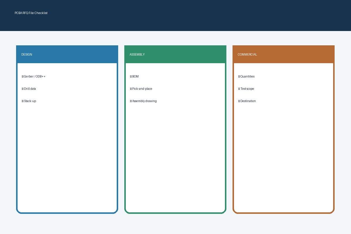
If your team is preparing a production quote, send the current Gerber or ODB++ data, drill files, fabrication drawing, BOM, pick-and-place file, assembly drawings, quantities, and test requirements through the PCB assembly quotation request. Ask that material exceptions and DFM dispositions be tied to the same revision before pricing is finalized.
How to evaluate fabrication findings
Fabrication findings should be reviewed against the finished geometry and the actual process sequence, not only the nominal CAD values. Copper imaging, etching, drilling, plating, solder-mask registration, routing, and lamination each contribute constraints.
- Trace width and spacing: confirm the affected layer, copper weight, finished requirement, and whether the flagged geometry is isolated or repeated.
- Annular ring and drill relationships: distinguish the design pad, drilled hole, finished hole, plating allowance, and registration allowance. The practical relationship is explained in this guide to PCB annular-ring and drill allowance.
- Board thickness and stack-up: check finished thickness tolerance, connector fit, dielectric construction, and impedance constraints. A thickness change can affect more than mechanical stiffness; review the PCB thickness selection factors before approving it.
- Copper-to-edge and slot clearance: identify whether the edge is routed, scored, plated, or mechanically constrained by an enclosure.
- Solder mask: inspect web width, registration, mask-defined features, exposed copper, and whether a requested expansion would alter fine-pitch pads.
- Controlled impedance: do not approve line-width or dielectric changes independently. Treat the stack-up, copper geometry, material family, finished copper, and impedance tolerance as one controlled decision.
When a supplier proposes a change, request both the adjusted value and the resulting finished condition. “Increase the pad” is incomplete if the report does not identify which pad, the target diameter, the affected clearances, and whether the change creates a new mask or spacing issue.

How to evaluate assembly findings
Assembly findings should connect land patterns and component data to the planned stencil, placement, reflow, through-hole, inspection, and test processes. A geometrically valid bare board can still create avoidable assembly risk.
- Land pattern and package match: compare the approved manufacturer part number, package drawing, footprint, polarity, pin-one convention, and centroid orientation.
- Stencil and paste distribution: review fine-pitch apertures, thermal-pad segmentation, nearby component height, and whether one stencil thickness can support the mixed feature set.
- Component spacing: consider placement nozzle access, rework tools, selective-solder fixtures, inspection sight lines, and mechanical hardware.
- Via treatment near pads: confirm whether vias are open, tented, filled, or capped and whether solder migration or planarity is relevant.
- Bottom-terminated components: decide how solder coverage and voiding will be evaluated and whether X-ray inspection is required.
- Testability: distinguish bare-board electrical test, AOI, X-ray, in-circuit test, programming, and functional test. Each method answers a different question.
IPC-7351 treats land patterns as part of a wider mounting condition that also includes solder mask, stencil, adjacent-component clearance, keepouts, and the attachment process. That is a useful reminder that a DFM response should not alter one geometry without checking its assembly context.
Placement-data quality is a frequent source of avoidable questions. Use the pick-and-place file preparation guide to align coordinates, rotation, side, designators, and the released BOM before the review begins.
Use a disposition matrix instead of approving by email
A disposition matrix creates an auditable decision for every finding. It should identify who owns the decision, what evidence was reviewed, whether files must change, and which revision contains the accepted result.
| Status | Use when | Required record |
|---|---|---|
| Accept supplier proposal | The change preserves design intent and requirements | Approved target value and revised-file owner |
| Approve as-is | The supplier confirms an acceptable process path | Documented exception and applicable build scope |
| Designer revision required | Electrical, mechanical, safety, or configuration intent changes | New controlled design release |
| Supplier clarification required | Location, rule, impact, or proposed action is incomplete | Specific question and requested evidence |
| Defer improvement | The note is advisory and does not block the current build | Future-action owner and rationale |
Never use a blanket statement such as “all DFM approved” when findings have different owners. A purchasing contact can acknowledge cost or schedule, but the appropriate engineering owner should approve changes to nets, stack-up, impedance, footprints, polarity, safety spacing, mechanical interfaces, or qualified materials.
Control the revised manufacturing package
After dispositions are complete, release one synchronized package. Do not send isolated replacement files without a manifest because the supplier may combine a new Gerber layer with an old drill file, drawing, BOM, or placement export.
- Increment the controlled revision according to the project’s change process.
- Regenerate fabrication and assembly outputs from the approved source design when possible.
- Check that filenames, drawing revision blocks, archive name, and manifest agree.
- Re-run output comparisons for copper, mask, paste, drill, profile, BOM, and placement data.
- Attach the closed disposition matrix and identify any approved supplier-specific exceptions.
- Require the quotation, order acknowledgment, and build traveler to reference the released revision.
If a supplier edits production data internally, request a description of the transformation and retain the customer-approved source package. Supplier working data should not become an undocumented replacement for design-controlled files.
Questions to ask when a DFM finding is unclear
Ask questions that expose the decision boundary rather than requesting a generic explanation.
- Which exact feature, layer, net, or reference designator triggered the rule?
- What value did the supplier measure, and what limit was used?
- Is the limit a quoted capability, a preferred process window, or a project requirement?
- What manufacturing or inspection outcome could occur if the design remains unchanged?
- Can the supplier build it as-is using a different process, and how would that affect cost, schedule, or evidence?
- Does the proposed change alter impedance, current capacity, isolation, mechanical fit, solder-joint geometry, or test coverage?
- Which released files must change, and who will regenerate them?
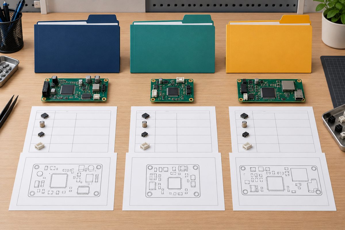
For a one-stop build, fabrication and assembly findings should be reviewed together. A bare-board change can affect stencil design, placement clearance, soldering, enclosure fit, or test fixtures. If you want one engineering review across fabrication, component sourcing, assembly, and test scope, submit the complete release package through the project quotation portal and identify the product revision and unresolved findings.
A practical pre-release checklist
The review is complete only when every finding has a disposition and the approved decision appears in a synchronized release package.
- Every finding has a unique identifier and reproducible location.
- Blockers, requirement conflicts, optimizations, and questions are separated.
- Electrical and mechanical design owners approved changes affecting design intent.
- Supplier capability statements are distinguished from contractual product requirements.
- Fabrication changes were checked for assembly and test consequences.
- BOM, placement data, drawings, stack-up, drill data, and image layers share one revision.
- Approved exceptions identify the supplier, process, revision, and build scope.
- The final quotation states the assumed materials, quantities, test scope, tooling, and open exclusions.
Turn DFM feedback into a controlled build decision
A PCB DFM report is valuable when it converts manufacturing knowledge into explicit engineering decisions. Treat each item as evidence to classify, reproduce, assess, and disposition. Approve changes only with the correct owner, then regenerate and verify the complete package. This approach reduces ambiguity without treating every supplier preference as a mandatory redesign.
When you are ready for a coordinated review, send the Gerber or ODB++ package, drill files, fabrication drawing, stack-up, BOM, pick-and-place data, assembly drawings, quantities, approved alternates, and test requirements through the OrinewPCB quotation form. The submission should identify unresolved DFM items so fabrication, sourcing, assembly, and testing assumptions can be reviewed against the same revision.
Latest Blog

Contact Info
Phone: +86-755-82882936
Email: [email protected]
WhatsApp: +86-13570802455
Wechat: +86-13570802455
Address: 2nd floor,D Bldg.,Electric Link Technology Bldg.,Gongming,Guangming New Dist.,518106 Shenzhen, China