
PCB Hipot Testing: Define Insulation Paths, Barriers, and Test Access
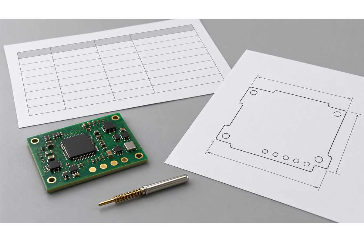
Table of Conent
Table of Conent
PCB hipot testing applies a specified high voltage across an intended insulation barrier while monitoring current, breakdown, or arcing according to an approved product or safety requirement. It is not a generic “high-voltage board test,” and it should never begin with an operator guessing which nets to connect. The engineering package must define each insulation path, which conductors are grouped on the high and return sides, test voltage type and level, ramp, dwell, trip criteria, discharge, product state, and required safety controls.
For a PCBA, the hardest work often occurs before the tester starts: identifying the real barrier through the schematic, layout, components, connectors, coating, chassis interfaces, and fixture. A controlled test map prevents skipped paths, overstressed low-voltage parts, unsafe residual charge, and results that cannot be traced to the released design.
What does a hipot test verify?
A hipot or dielectric-withstand test provides evidence that a specified insulation barrier withstands the applied electrical stress for the required conditions without prohibited breakdown or excessive current. It differs from continuity, insulation-resistance, leakage-current, ground-bond, and functional tests. Those methods answer different questions and may all appear in one product safety plan.
| Test | Primary question | Why it is not interchangeable |
|---|---|---|
| Hipot / dielectric withstand | Does the defined barrier withstand the specified electrical stress? | May stress insulation and uses defined trip behavior |
| Insulation resistance | What resistance exists across a barrier at the specified test condition? | Normally uses different limits and interpretation |
| Protective-earth continuity | Is the required low-resistance bonding path intact? | Checks a conductor, not insulation separation |
| Functional test | Does the assembly perform the required operation? | Does not establish dielectric withstand |
Chroma describes dielectric strength testing as applying AC or DC voltage across insulation while monitoring leakage, breakdown, or arc behavior. The applicable product standard or customer specification must define the actual method. Do not reuse a common “two times working voltage plus 1,000 V” rule unless the governing requirement explicitly calls for it.
How do you define the insulation-path test matrix?
Start with electrical safety boundaries, not board layers. Identify hazardous circuits, SELV or other low-voltage circuits, protective earth, chassis, accessible conductive parts, isolated communications, transformer windings, relay contacts, and external connectors as applicable. For each required test, specify which nodes are tied together on each side of the barrier and which components are connected, disconnected, shorted, or bypassed.
A useful matrix includes the path identifier, barrier description, high-side node group, return-side node group, board and BOM revision, product switch state, connector condition, applied waveform, voltage, ramp, dwell, current or arc limit, discharge requirement, standard clause, and pass/fail record. A schematic highlighted with color can support the matrix, but color alone is not machine-readable control.
The PCB test-point design guide explains why electrical intent, physical access, probe geometry, and product stage must be reviewed together. Hipot access adds high-voltage clearance, fixture insulation, guarding, and discharge concerns beyond ordinary low-voltage probing.
Which PCB features can bridge or weaken the intended barrier?
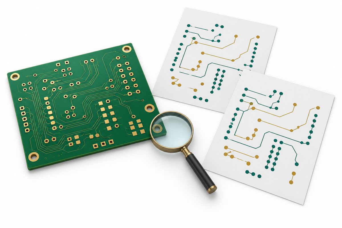
Review the finished physical construction, not only schematic isolation. Copper spacing, slots, cutouts, solder mask, plated holes, component pads, mounting hardware, shields, heatsinks, connectors, contamination, adhesives, coating, and enclosure interfaces can change the effective path. A barrier that appears clear on one copper layer may be crossed by a via, inner-layer plane, component body, or assembly material.
Creepage and clearance requirements depend on the applicable standard, working voltage, overvoltage category, pollution degree, material group, altitude, coating qualification, and other product conditions. Do not quote a universal spacing without those inputs. Fabrication tolerances and assembly variation must also leave the finished product compliant, not merely the nominal CAD geometry.
Before requesting a build, submit Gerbers, stackup, schematic, BOM, assembly drawings, isolation requirements, quantities, and test matrix through the PCB assembly engineering review path. This allows fabrication, component sourcing, assembly, fixture, and electrical-test assumptions to be reviewed together.
How should components be treated during the test?
Some components intentionally bridge an insulation boundary: transformers, optocouplers, Y capacitors, relays, filters, surge devices, or isolation amplifiers. Others may be damaged if the test connects voltage across pins or semiconductor structures that were not intended to withstand it. The test state must follow the product standard, component ratings, and approved circuit analysis.
Document whether switches are open or closed, line and neutral are tied, capacitors are charged, surge suppressors are connected, relays are energized, connectors are mated, or removable modules are present. Never improvise by lifting components or cutting traces on production units unless an approved procedure explicitly requires and restores that condition.
DC testing can charge capacitive structures. The fixture and sequence need a verified discharge step and a safe indication before access. AC testing creates reactive current that can influence the measured value. Selection between AC and DC is a standards and design decision, not simply a preference for the tester with the higher available voltage.
If component ratings or isolation states remain unclear, send the schematic, BOM, barrier map, board files, required standard, and planned production quantity through the engineering quotation review. The review can identify missing approvals before fixture wiring or high-voltage testing begins.
What test access and fixture controls are required?
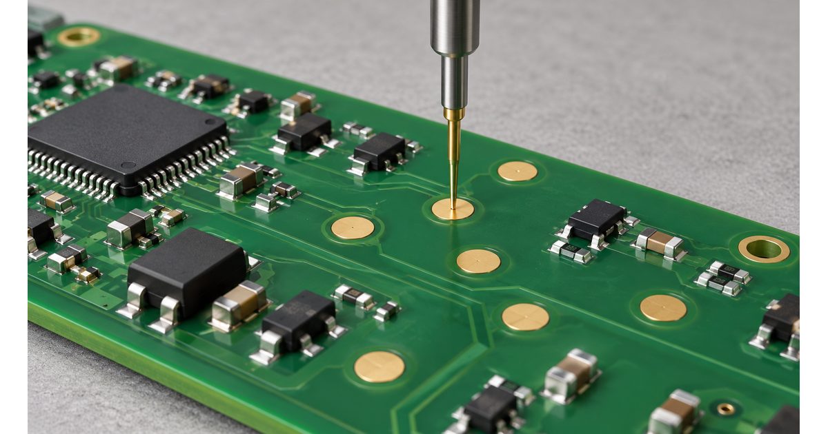
Test points and connectors should let the fixture contact the intended node groups without exposing personnel or applying stress to unintended circuits. Use rated wiring, probes, relays, connectors, insulation, spacing, barriers, and interlocks for the maximum test condition. The fixture must prevent a low-voltage channel, programmer, functional tester, or grounded instrument from becoming an unintended current path.
Define contact sequence and verify the fixture is fully engaged before high voltage is enabled. Guarded enclosures, two-hand controls, light curtains, door interlocks, warning indicators, emergency stops, and automatic discharge may be appropriate depending on the station and risk assessment. Keysight’s service guidance warns that dielectric-withstand testing presents hazards to personnel and property and should be performed only by knowledgeable people under controlled conditions.
A fixture validation should include point-to-point wiring checks, insulation verification, interlock challenge, open/short or connection checks, known pass/fail samples where appropriate, software revision, and safe recovery after power loss or aborted tests.
How are ramp, dwell, current limits, and discharge specified?
Use the governing requirement and qualified engineering procedure. The ramp controls how quickly stress is applied and can reduce unnecessary transients or nuisance trips. Dwell defines how long the specified level is maintained. Current and arc criteria distinguish acceptable charging or reactive behavior from a prohibited event. Discharge defines when the device is safe to handle.
Capacitance, filters, cable length, fixture construction, humidity, contamination, and connected components can influence measured current. Establish limits with the actual product and validated method. Do not raise a trip limit merely to make a failing unit pass; first separate normal capacitive behavior, fixture leakage, contact instability, contamination, and genuine insulation failure.
Chroma’s practical dielectric-testing guidance describes gradual voltage ramping, monitored current, programmed duration, automatic shutdown on an excessive-current condition, and discharge before disconnection. Those principles still require project-specific values from the applicable requirement.
What is the difference between development and production testing?
Development testing characterizes the design, margin, materials, and failure mechanisms; production testing screens workmanship against an approved process. A destructive design-limit experiment should not be copied directly into every production unit. Conversely, a shorter production test must come from the governing standard and validated plan, not from schedule pressure.
Define whether the test applies to every unit, a sample, first article, lot, repaired product, or design qualification. Record the board revision, fixture, tester, program, applied parameters, measured result, failure code, operator or station identity, date, and disposition. If the assembly is integrated into an enclosure, confirm whether the PCB-level test is sufficient or whether the final product needs a separate safety test.
The flying-probe versus bed-of-nails comparison covers structural production testing and lifetime cost. Those methods may detect opens or shorts, but they do not automatically provide the rated insulation, guarding, or procedure required for hipot.
How should failures and retests be handled?
A hipot failure is a high-energy event that may alter the unit. Stop, discharge, isolate, and preserve evidence. Record the exact path, applied voltage at failure, current or arc indication, time, fixture state, environmental condition, and visible evidence. Do not repeatedly retest at full voltage until the unit passes; repeated stress can carbonize a path, damage a component, or erase the original cause.
First determine whether the failure belongs to the product or the test system. Check fixture cleanliness, wiring, damaged probes, humidity, contamination, connector seating, and program revision using a safe approved diagnostic sequence. Product investigation may examine residues, spacing, damaged insulation, component mix, coating, hardware, solder debris, board defects, or handling damage.
Define the authority for rework, retest, concession, and scrap. A repaired barrier should receive the required inspection and test under the approved procedure, and the record should link the original failure to the final disposition.
How do contamination and coating affect the result?
Flux residues, process chemicals, fibers, dust, moisture, fingerprints, solder balls, and conductive debris can create leakage or tracking paths. A test failure may reveal a cleaning or handling problem, but a pass does not prove long-term cleanliness or resistance to the field environment. Ionic contamination and surface-insulation testing answer different questions.
Conformal coating can support environmental protection when correctly selected, applied, cured, and qualified, but it should not be treated as an automatic substitute for required spacing. Masking boundaries, bubbles, thin edges, contamination under coating, and repair areas can influence the barrier. Specify whether hipot occurs before coating, after coating, after enclosure assembly, or at several stages.
The PCB assembly process guide helps place electrical safety testing within fabrication, cleaning, coating, inspection, and final functional verification.

Pre-release PCB hipot checklist
- Applicable product standard and exact clause identified.
- Every insulation path mapped to controlled node groups.
- AC or DC method, voltage, ramp, dwell, trip, and discharge defined.
- Component states and temporary connections documented.
- Finished PCB spacing, slots, materials, coating, and hardware reviewed.
- Fixture voltage rating, guarding, interlocks, and safe sequencing validated.
- Tester calibration and program revision controlled.
- Production sampling, records, failure codes, and retest authority defined.
- Post-test discharge verified before operator access.
- Gerbers, schematic, BOM, drawings, quantities, and safety requirements agree.
PCB hipot testing is reliable only when the insulation boundary and test state are explicit. Map the path, protect unintended circuits, validate the fixture, control hazardous energy, and keep every result tied to the released product. For a one-stop PCBA review, provide the fabrication package, schematic, BOM, assembly drawings, safety requirements, test matrix, quantities, and reporting needs through the RFQ page. The engineering review can then scope PCB fabrication, component sourcing, assembly, cleaning or coating, fixture development, electrical safety testing, functional testing, and delivery.
Technical references: Chroma electrical safety testing overview and Keysight service guidance with dielectric-withstand safety precautions.
Latest Blog

Contact Info
Phone: +86-755-82882936
Email: [email protected]
WhatsApp: +86-13570802455
Wechat: +86-13570802455
Address: 2nd floor,D Bldg.,Electric Link Technology Bldg.,Gongming,Guangming New Dist.,518106 Shenzhen, China