
0.5 mm PCB Thickness: Managing Warpage and Assembly Limits
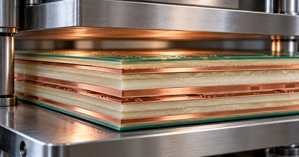
Table of Conent
Table of Conent
A 0.5 mm PCB can solve a real enclosure or weight constraint, but the thickness should be treated as a controlled mechanical and assembly requirement—not as a simple reduction from a standard board. A thin rigid board has less bending stiffness, making copper balance, stackup symmetry, panel support, handling, paste printing, placement, reflow, depanelization, connector loading, and finished thickness tolerance more important.
The right question is not only whether a fabricator can make a 0.5 mm board. It is whether the board, production panel, assembly process, and finished product can remain flat and mechanically stable enough for the selected components, fixtures, connectors, and test method. Confirm those limits with both the bare-board fabricator and assembler before layout release.
What does 0.5 mm PCB thickness specify?
State whether 0.5 mm is the nominal finished thickness and define the permitted tolerance in the procurement documentation. Finished thickness includes the laminated dielectric and copper structure and may be affected by plating and surface buildup according to the supplier’s measurement practice. Do not assume that a catalog core marked 0.5 mm produces a 0.5 mm finished multilayer board.
Thickness also affects enclosure slots, board-to-board connector engagement, press-fit or card-edge interfaces, screw stackups, thermal contacts, shielding, and fixture clamping. Identify the measurement locations and any keepout or local buildup that matters to fit. If the mechanical system only works within a tight range, make that requirement explicit rather than relying on a general factory tolerance.
| Decision | Why it matters at 0.5 mm | Evidence to approve |
|---|---|---|
| Finished thickness and tolerance | Controls fit, stiffness, and process capability | Fabrication drawing and supplier confirmation |
| Layer count and copper weights | Influence symmetry, routing, and dimensional stability | Approved production stackup |
| Panel and support strategy | Limits sag during printing, placement, and reflow | Assembly panel drawing and fixture plan |
| Bow and twist acceptance | Affects print gasketing, placement, joints, and fit | Measurement method and acceptance record |
| Mechanical loading | Thin boards flex more under connectors and handling | Product-level mechanical verification |
Confirm that a thin rigid board is the right architecture
A 0.5 mm rigid PCB is not interchangeable with a flexible circuit. A thin FR-4 board can bend more than a conventional rigid board, but repeated dynamic flexing can damage copper, plated holes, solder joints, and components. If the product requires repeated motion, use a flex or rigid-flex architecture designed and qualified for that motion.
Choose 0.5 mm because the mechanical envelope, mass, connector, optical path, or product architecture needs it. If thickness is merely assumed to reduce cost, check the full quotation. Nonstandard materials, tighter handling controls, special panels, carriers, fixtures, yield loss, and inspection can outweigh the laminate savings.
Large outlines, long narrow shapes, edge connectors, heavy components, and unsupported cables increase mechanical risk. Model or test the assembled board under installation, service, vibration, shock, connector insertion, and handling loads relevant to the product.
Build a symmetric, manufacturable stackup
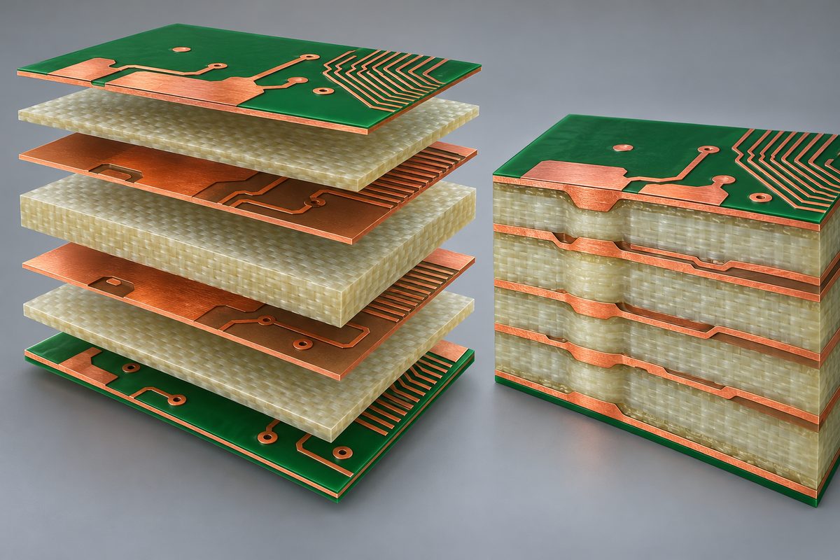
For a multilayer 0.5 mm board, layer count and dielectric spacing are constrained. Keep the construction as symmetric as practical about the centerline, including copper weights and dielectric distribution. Large copper imbalance between opposite layers can create unequal stress during lamination, etching, and thermal cycling.
Copper balancing does not mean filling every empty area without review. Added copper can change impedance, creepage, antenna behavior, capacitance, heat flow, and isolation. The design team and fabricator should agree on thieving or balancing features and identify areas where they are prohibited.
Use named materials or controlled equivalent-property criteria when electrical, thermal, or reliability performance matters. Review glass style, resin system, copper foil, Tg, Z-axis expansion, moisture behavior, and the ability to meet the proposed dielectric and finished-thickness tolerances. The PCB lamination guide explains how resin flow, copper distribution, moisture, press control, and material construction affect final thickness and planarity.
Design holes and vias for the actual thin-board process
A thin finished board can offer a favorable through-hole aspect ratio, but that does not remove annular-ring, registration, plating, breakout, and handling requirements. Define finished holes, drill sizes where required, pad diameters, tolerances, plating expectations, and any microvia structure with the supplier.
Avoid weakening narrow regions with dense perforations, closely spaced slots, or poorly supported breakaway tabs. Vias near the edge, large cutouts, and connector openings can create local flex concentrations. Review copper-to-edge clearance and routing tolerances, especially where the thin board will be inserted into a housing or card guide.
For controlled-impedance routing, confirm the production stackup before fixing trace widths. Very thin dielectrics may require narrow or otherwise sensitive geometries depending on the reference arrangement. Include material, layer, reference plane, target impedance, and tolerance in the release package.
Plan the production panel for stiffness and handling
The assembly line normally handles a panel or array, not a loose 0.5 mm unit. Rails, tooling holes, fiducials, breakaway structure, and support locations should be designed with the assembler. A panel that is too large or has insufficient rails may sag under its own weight or respond unevenly to conveyor support and heating.
Panel layout should keep copper and thermal mass reasonably balanced, provide support under pressure and placement zones, and avoid placing fragile components beside depanelization features. Confirm whether V-scoring is suitable for the thickness, outline, copper clearance, and component distance. Routed tabs may provide better control for some shapes, but tab location and residual nib removal need review.
Do not optimize material utilization independently of assembly stability. A dense panel can reduce bare-board waste while making paste printing, transport, reflow support, inspection, or depanelization unreliable. Quote both fabrication and assembly using the same panel revision.
Support the board during solder-paste printing
Printing requires the PCB to contact the stencil consistently. If a thin panel deflects under squeegee force, paste volume and aperture release can vary. Tooling should support the panel without interfering with bottom-side features. Dedicated support pins, vacuum tooling, a machined carrier, or other approved support may be appropriate.
Verify board and stencil cleanliness, clamping, support height, print pressure, separation settings, and solder-paste inspection results. Fine-pitch and bottom-terminated components are particularly sensitive because small changes in paste deposit can affect opens, bridges, voiding, or component float.
The goal is not to clamp the board so aggressively that it stores stress and springs back after printing. Support should establish a repeatable print plane while respecting components or features on a second assembly side.
Control placement and reflow without unsupported assumptions
Placement equipment needs a stable datum. Thin panels may vibrate, flex under nozzle force, or shift if support and clamping are inadequate. Review component mass, nozzle force, placement sequence, board support, and fiducial strategy. Large or heavy parts may need special consideration even when small passives place normally.
During reflow, temperature gradients, copper imbalance, component mass, panel orientation, conveyor support, and material behavior can change board shape. Use a product-representative thermal profile and support arrangement. A carrier can help, but it also changes heating and cooling, so profile the assembly in its actual tooling rather than copying an unsupported-board recipe.
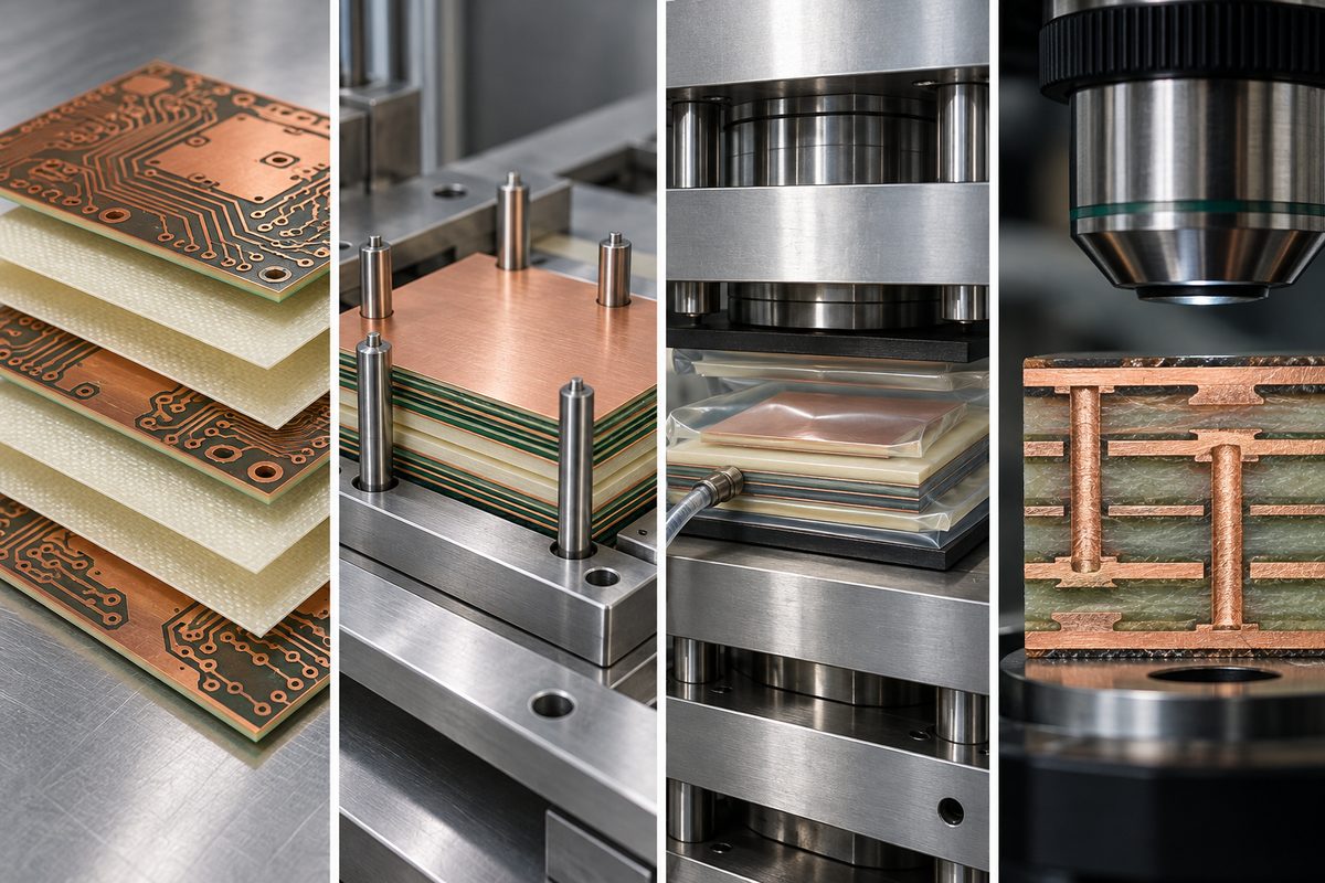
The PCB assembly process guide connects incoming board checks, printing, placement, reflow, inspection, through-hole operations, and testing. For a 0.5 mm build, document where special support is required at each step.
Measure bow and twist at the relevant stages
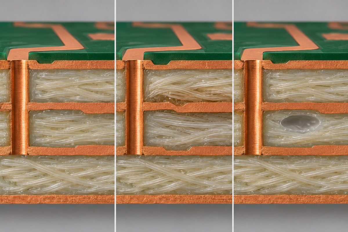
Define bow and twist requirements in the purchase specification and identify the applicable standard and revision. IPC technical resources discuss physical measurement using IPC-TM-650 methods and show why thin-board qualification must consider both finished-board geometry and assembly exposure. Do not copy a percentage from a different product class without confirming the contractual requirement.
Measure at agreed stages: as-received bare board, after moisture conditioning or bake if required, after representative reflow cycles, after depanelization, and after final assembly where product fit depends on it. Record the specimen condition, support, temperature, panel or unit state, and measurement method.
A board can meet incoming flatness and still distort during reflow. Conversely, a panel may relax after depanelization. The acceptance plan should reflect the stage that affects paste printing, component joints, connector fit, enclosure assembly, or product function.
Protect the board during depanelization and final assembly
Thin boards can flex sharply during manual tab breaking or poorly supported routing. Select a depanelization method that controls strain, and locate components, solder joints, ceramic packages, and sensitive traces away from high-strain areas. Use fixtures where needed and define acceptable residual tab material.
Connector insertion, screw tightening, heat-sink attachment, cable strain, conformal coating, potting, and enclosure clamping can all bend a 0.5 mm PCB. Use mechanical stops, spacers, stiffeners, brackets, or housing support where the product design requires them. Torque specifications and assembly sequence should prevent the enclosure from forcing the board flat against an incompatible surface.
Testing fixtures also need review. Bed-of-nails pressure, pogo-pin count, vacuum pull-down, edge clamping, and connector actuation can deform a thin board. Support near probe fields and loaded connectors without masking the defects the test is supposed to detect.
Specify inspection and validation beyond thickness alone
Incoming inspection should verify revision, material documentation where required, thickness, outline, holes, surface finish, solder mask, markings, flatness, visible damage, and electrical-test status. Sampling, traceability, and records should match the product risk and purchase agreement.
After assembly, use AOI for visible placement and solder features, X-ray where joints are hidden, solder-paste inspection where print stability is critical, and functional or in-circuit testing appropriate to coverage. Inspect panel position trends because edge and center units may experience different support or thermal conditions.
Run a prototype or pilot lot with production-intent panels, tooling, paste, profile, and inspection. A hand-assembled loose board does not validate automated handling. The PCB DFM report workflow helps turn thickness, panel, copper-balance, tooling, and depanelization findings into controlled decisions before volume production.
What should a 0.5 mm PCB RFQ include?
Provide Gerber or ODB++ data, drill files, fabrication drawing, nominal finished thickness and tolerance, material and copper requirements, stackup, impedance table if applicable, outline and panel data, bow and twist criteria, surface finish, solder mask, quantity, BOM, placement file, assembly drawings, component height and mass concerns, stencil requirements, support or carrier assumptions, reflow constraints, depanelization method, inspection, test, and delivery requirements.
For an early feasibility review, send the outline, proposed layer count, target thickness, copper weights, component map, mechanical fit constraints, expected assembly sides, and quantities through the thin PCB engineering quotation path. Ask the fabricator and assembler to respond against the same revision.
For a pilot build, use the PCB assembly RFQ page to define production-intent panelization, tooling, reflow support, inspection, sample size, and the evidence required before release.
0.5 mm PCB release checklist
- State nominal finished thickness, tolerance, and measurement expectations.
- Confirm enclosure, connector, stiffener, and fixture interfaces.
- Use a symmetric stackup and review copper balance without compromising electrical intent.
- Confirm materials, dielectric construction, holes, vias, and impedance geometry.
- Approve panel rails, fiducials, support, breakaway structure, and depanelization.
- Validate printing support, placement stability, and production-intent reflow tooling.
- Define bow and twist requirements, method, and measurement stages.
- Review connector, screw, cable, coating, potting, and test-fixture loads.
- Use prototype or pilot lots with production-intent panels and processes.
- Keep fabrication, assembly, inspection, and test data under one revision.
A 0.5 mm PCB is successful when the whole manufacturing route is designed for a thin structure. To coordinate stackup engineering, fabrication, component sourcing, assembly carriers, inspection, testing, and delivery, submit the controlled package through the AssyPCB RFQ page. The useful outcome is not merely a board measured at 0.5 mm; it is an assembled product that remains processable, testable, and mechanically fit for its intended use.
Technical references: IPC technical paper on thin form-factor PWB qualification, IPC technical paper on board warpage during reflow, and IPC-6012EA table of contents and acceptance references.
Latest Blog

Contact Info
Phone: +86-755-82882936
Email: [email protected]
WhatsApp: +86-13570802455
Wechat: +86-13570802455
Address: 2nd floor,D Bldg.,Electric Link Technology Bldg.,Gongming,Guangming New Dist.,518106 Shenzhen, China