
High-Speed PCB Design: Manage Transmission Lines and Signal Integrity
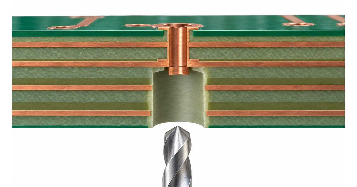
Table of Conent
Table of Conent
High-speed PCB design begins when a signal’s transition time makes the interconnect behave as a transmission line, not when a marketing label reaches a particular clock frequency. The practical task is to preserve a controlled path from driver to receiver: define the interface requirement, select a manufacturable stackup, control impedance, provide a continuous return path, minimize discontinuities, manage coupling and loss, and verify the finished channel against the product’s timing and noise margins.
A layout rule such as “route at 100 ohms” is only one part of that system. The package, launch, trace, vias, connector, cable, termination, receiver, power distribution, and fabrication tolerances all contribute. The most useful release package therefore connects electrical intent to geometry the PCB fabricator can build and evidence the assembly and test teams can verify.
What makes a PCB signal high speed?
Rise and fall time are usually more important than the nominal clock rate. A low-frequency signal with a very fast edge can excite reflections on a route that would be electrically short for a slower edge. Treat a route as a possible transmission line when its propagation delay is no longer negligible compared with edge time. The exact boundary depends on the driver, loading, interconnect, acceptable distortion, and design margin.
Classify critical nets before placement. Include clocks, fast single-ended buses, differential serial links, memory interfaces, sensitive analog paths, switching nodes, and any signal whose timing, jitter, overshoot, crosstalk, or emissions can affect compliance. Use interface and component documentation for the applicable topology and limits instead of applying a generic rule to every net.
| Input | Decision it supports | Release evidence |
|---|---|---|
| Edge rate, voltage, load, and topology | Transmission-line and termination strategy | Interface requirement and simulation model |
| Target impedance and tolerance | Stackup and trace geometry | Controlled-impedance table |
| Timing and loss budget | Length, layer, via, and material limits | Constraint report and channel analysis |
| EMI and crosstalk limits | Spacing, reference planes, and shielding | Layout review and test plan |
Start with the stackup, not the final routed board
Every critical signal layer needs a defined reference plane. The dielectric thickness, trace width, copper thickness, material properties, solder mask, and whether the route is microstrip or stripline affect impedance. Ask the fabricator to confirm a production stackup before detailed routing; substituting a core or prepreg after layout may force geometry changes or shift the predicted result.
Specify the target as single-ended or differential impedance, identify the routed layer and reference plane, state the tolerance, and define which structures require coupons or test results. Do not copy a trace width from a different stackup. Catalog dielectric constant is not always the effective value at the relevant frequency and construction, and pressed prepreg thickness depends on resin flow and copper distribution.
The 10-layer PCB stackup guide shows how signal layers, ground planes, power distribution, BGA escape, and via planning interact in a dense design. A lower or higher layer count can work, but extra layers only help when their assignments preserve reference paths and manufacturable geometry.
Protect the complete return-current path
A signal route and its return form one electromagnetic structure. At high frequency, return current concentrates near the signal on the adjacent reference plane. Routing over a plane split, slot, void, or large anti-pad forces the return to detour, increasing loop area and creating an impedance discontinuity and potential radiation source.
Texas Instruments’ high-speed layout guidance recommends continuous reference planes and warns against routing high-speed signals across plane splits. At a layer transition, provide an appropriate nearby return path. When both layers reference ground, stitching vias close to the signal transition can reduce the return detour. If references change between ground and power, the transition needs deliberate AC return planning compatible with the power system.
Do not add stitching features mechanically. Their location, spacing, drill structure, plane connection, and interaction with anti-pads matter. Review connector grounds and cable shields as part of the path; a beautifully routed trace can still encounter a poor launch or return discontinuity at the board edge.
Control impedance without treating it as a magic number
Impedance control reduces reflections when the source, line, load, and termination strategy are compatible. For a differential pair, both the individual trace relationship to the reference plane and the coupling between the traces contribute. The target value comes from the interface requirement, not from a universal preference.
Keep geometry consistent through straight segments, bends, breakouts, and neck-down regions. Where the route must narrow at a package or connector, minimize the discontinuity and include it in channel analysis when margins are tight. Copper etch, plating, trace trapezoid, dielectric tolerance, solder mask, and local plane openings can move the manufactured impedance from the nominal CAD calculation.
Specify how the fabricator should report controlled impedance and whether a test coupon represents the critical construction. Coupon results verify the coupon and process sample; they do not directly measure every routed channel. For high-risk products, combine coupon evidence with stackup verification, artwork review, and channel-specific analysis or measurement.
Route differential pairs for symmetry and a valid reference
Differential routing depends on more than matching total lengths. Keep the two conductors on the same layer where practical, maintain consistent spacing and reference geometry, use comparable bends and vias, and avoid asymmetric pads or stubs. Correct local skew near the source of mismatch rather than adding long serpentine sections far away without considering coupling and loss.
Use the component or interface vendor’s current limits for intra-pair skew, inter-pair timing, impedance, spacing, and via count. TI’s guidance for high-speed interfaces emphasizes adjacent ground reference, controlled differential impedance, limited vias, and avoidance of split planes. Those are interface-specific starting points, not permission to reuse one numeric rule for every protocol.
Separate pairs and other aggressors according to the crosstalk budget and stackup. A simple three-times-width spacing rule can be a screening guideline, but field solvers or channel simulation are more appropriate when density, long parallel runs, broadside coupling, or tight margins dominate.
Manage vias, stubs, connectors, and other discontinuities
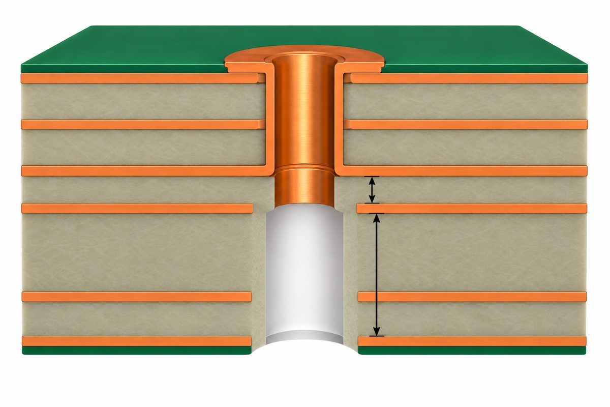
A via adds inductance and capacitance, and an unused barrel section can behave as a resonant stub. The effect depends on stub length, signal spectrum, anti-pad, pad stack, reference transition, via spacing, and surrounding copper. Minimize unnecessary transitions, but do not assume that any via automatically fails a high-speed design.
Use layer assignment to shorten through-via stubs where possible. For channels that require it, consider blind vias, optimized anti-pads, nonfunctional-pad removal, or backdrilling. Each option changes fabrication cost and risk. Intel’s board-design guidance notes that unused via pads add capacitance, while TI explains how via geometry, shared anti-pads, return vias, and backdrilling influence differential transitions.
The PCB backdrilling guide explains how to define entry side, protected connections, residual-stub requirements, drill clearance, and verification. Do not specify “backdrill as needed”; identify exactly which vias, layers, and residual conditions the fabricator must meet.
Model connector launches, AC-coupling pads, test points, ESD devices, and package breakouts where they dominate the channel. A test pad placed as a branch can create a stub. Prefer inline or purpose-designed probing structures when signal-integrity requirements allow, and coordinate access with the actual test method.
Control crosstalk, loss, and timing as separate budgets
Crosstalk depends on coupling length, spacing, layer geometry, reference integrity, edge rate, and whether aggressors switch together. Separate sensitive nets from switching power nodes, clocks, and unrelated high-speed channels. Avoid long parallel runs on adjacent layers unless the stackup and orientation are designed for it.
Insertion loss grows with conductor and dielectric loss, route length, vias, connectors, and frequency. Material selection should follow the actual channel loss budget, not the assumption that every fast interface requires an exotic laminate. Short channels may work on a controlled FR-4 system; longer or faster channels may require lower-loss material and tighter process control.
Timing review includes propagation delay, intra-pair skew, bus matching, package delay, via delay, connector delay, and receiver setup or sampling margin. Matching copper length alone can be misleading if routes use different layers, glass-weave environments, via counts, or connector paths. Match the electrical path that the interface cares about.
Plan power integrity and decoupling with the signal path
Signal integrity and power integrity are connected. Driver current transitions draw energy from the power distribution network, and supply noise can become timing jitter or common-mode noise. Place decoupling for short, low-inductance current loops, use suitable plane relationships, and review anti-resonance and target impedance where system risk warrants it.
Keep switching-converter hot loops and high-dV/dt nodes away from sensitive signals. Return-path continuity does not mean routing every function through one congested region; placement should organize functional blocks so that high-current and high-frequency fields do not interfere with receivers, clocks, references, or analog conversion paths.
Analog Devices’ layout guidance for high-speed converters emphasizes placement, exposed-pad grounding, short bypass connections, and solid reference planes. Apply the device vendor’s recommendations to the actual component rather than relying on a generic decoupling count.
Use simulation and measurement that match the decision
Pre-layout analysis can establish stackup, termination, spacing, and topology rules. Post-layout extraction can include the routed geometry, vias, connectors, and package models. Select models with known scope and validity, and document assumptions. A simulation result is not evidence if the production stackup or installed components differ from the model.
Verification may include impedance coupons, time-domain reflectometry, eye diagrams, bit-error testing, oscilloscope measurements, spectrum analysis, or product functional stress tests. Define fixtures, probe bandwidth and loading, calibration or de-embedding method, test pattern, operating conditions, and acceptance criteria before measuring.
Do not interpret one clean waveform at room temperature as complete qualification. Include relevant voltage, temperature, process, cable, connector, and data-pattern corners according to product risk. Conversely, do not require every possible instrument test without a failure mechanism or decision it supports.
Release fabrication and assembly data as one controlled package
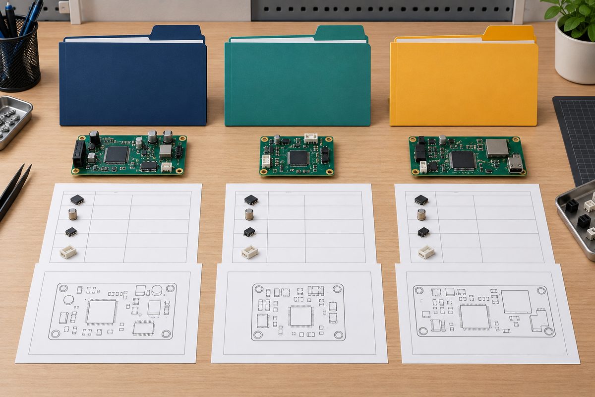
A high-speed PCB release should include Gerber or ODB++ data, drill and backdrill files, approved stackup, material or equivalent-property requirements, impedance table, controlled-net list, layer references, via structures, fabrication drawing, coupon requirements, BOM, placement data, assembly drawings, programming instructions, inspection and test requirements, quantities, and revision history.
Use the PCB DFM report guide to classify findings, resolve conflicts, and preserve approved dispositions. Fabrication cannot safely “optimize” a trace, anti-pad, dielectric, or via without understanding the electrical constraint behind it.
For early stackup and channel review, submit the preliminary layer plan, material constraints, interface types, impedance targets, estimated lengths, via strategy, and target quantities through the PCB engineering quotation path. Resolve manufacturability before the geometry becomes expensive to change.
For a turnkey build, use the PCBA RFQ page to include bare-board requirements, BOM, placement data, assembly details, controlled substitutions, programming, inspection, functional-test scope, and delivery conditions. That lets fabrication and assembly decisions be reviewed together.
High-speed PCB release checklist
- Classify critical nets from edge rate, topology, timing, noise, and compliance risk.
- Approve a manufacturable stackup before detailed routing.
- Define impedance targets, tolerances, layers, references, and coupon expectations.
- Keep return paths continuous and plan every layer transition.
- Preserve differential-pair symmetry and interface-specific skew limits.
- Review via stubs, anti-pads, connectors, test structures, and package breakouts.
- Budget crosstalk, insertion loss, reflections, and timing separately.
- Coordinate power integrity, decoupling, placement, and high-current loops.
- Run pre-layout and post-layout analysis appropriate to the channel risk.
- Define measurement fixtures, conditions, and acceptance criteria.
- Reconcile fabrication, assembly, programming, inspection, and test revisions.
High-speed design succeeds when electrical intent survives physical implementation and production variation. To coordinate stackup engineering, controlled-impedance fabrication, component sourcing, assembly, inspection, and channel verification in one workflow, send the complete controlled package through the AssyPCB RFQ page. The objective is not merely a routed board; it is a repeatable assembled product with evidence that its critical interfaces meet the defined limits.
Technical references: Texas Instruments High-Speed Layout Guidelines, Intel AN 958 Board Design Guidelines, and Analog Devices AN-1177 LVDS and M-LVDS Circuit Implementation Guide.
Latest Blog
Contact Info
Phone: +86-755-82882936
Email: [email protected]
WhatsApp: +86-13570802455
Wechat: +86-13570802455
Address: 2nd floor,D Bldg.,Electric Link Technology Bldg.,Gongming,Guangming New Dist.,518106 Shenzhen, China