
ARINC 429 Interface Board Changes: When a Patch Requires a Respin
Table of Conent
Table of Conent
An ARINC 429 interface-board patch is acceptable only when the changed hardware, installation, manufacturing process, verification evidence, and approval basis remain clearly controlled. A wire, component substitution, protection-device change, or layout repair may restore one bench function while changing impedance, return paths, creepage, lightning-current routing, thermal behavior, vibration durability, configuration identity, or production repeatability.
Decide between a controlled patch and a PCB respin by tracing the change to requirements and failure mechanisms. Preserve the original evidence, define the exact modification, assess electrical and physical consequences, determine which analyses and tests are affected, and release a configuration that manufacturing can reproduce. Do not describe an interface board as “DO-160 qualified” without identifying the tested equipment configuration, environmental categories, test levels, procedures, and approved evidence.
First define the problem, not the proposed patch
Record the observed symptom, board and assembly revision, serial number or lot, installed equipment configuration, software or FPGA version, cable and load, power condition, temperature, test setup, and the point in the lifecycle where the issue appeared. Separate a schematic design error from a layout problem, assembly defect, component issue, software configuration, test-fixture artifact, or installation problem.
For an ARINC 429 channel, identify whether the problem affects transmit amplitude or waveform, rise and fall behavior, receiver threshold margin, label or parity handling, timing, channel isolation, common-mode behavior, protection, power consumption, emissions, susceptibility, or mechanical integrity. A generic “bus failure” does not give reviewers enough information to judge the remedy.
| Change example | Patch may be reviewable when | Respin is favored when |
|---|---|---|
| Series resistor or termination correction | Short controlled rework has known parasitics and repeatable placement | The network or current path must be redesigned |
| Trace cut and jumper | One evaluation unit needs a documented reversible experiment | Field, production, EMI, vibration, or spacing performance depends on the route |
| Protection-device replacement | Footprint and circuit requirements remain compatible and evidence is updated | Energy path, capacitance, clamping, clearance, or qualification basis changes |
| Transceiver substitution | The exact candidate is approved with appropriate comparison and verification | Pinout, supplies, waveform, protocol behavior, package, or thermal design changes |
| Connector or shield change | Mechanical and return connections remain equivalent and controlled | Installation interface or current-return architecture changes |
Understand what the ARINC 429 interface contains
An interface can include a protocol controller, transmitter and receiver functions, line drivers, level translation, isolation where required by the design, filters, protection devices, resistive networks, connectors, shields, power conversion, discrete controls, and built-in-test routing. Some devices integrate several functions; others use separate analog and digital components.
Use the exact component data sheets and the program’s applicable ARINC specification rather than relying on a general description. Holt and Data Device Corporation publish multiple ARINC 429 controllers, drivers, receivers, and evaluation hardware with different channel counts, supply needs, packages, protection features, test modes, and interfaces. Similar function names do not establish drop-in interchangeability.
Map the channel from processor or FPGA pins through the physical-layer circuitry to the connector and installed harness. Include power and return paths. A patch near the controller may alter digital timing; a change near the line interface may alter waveform, common-mode, protection, or emissions behavior.
When is a patch useful?
A patch is valuable for fault isolation, hypothesis testing, prototype learning, or a narrowly controlled engineering evaluation. Examples include removing a suspect branch, changing one passive value, adding a temporary test connection, or substituting a candidate device on a limited sample. The patch should answer a defined question and preserve the ability to compare against the original configuration.
Specify the wire type, gauge, insulation, route, maximum length, attachment points, soldering method, strain relief, adhesive if permitted, clearance from other conductors, workmanship criteria, inspection, and rework authority. Photographs are useful but do not replace a drawing and written instruction.
A successful patched unit does not automatically authorize fleet, field, or production use. State whether the configuration is laboratory-only, test-only, prototype, limited-production, or approved for a defined scope. Prevent patched and unpatched units from being mixed without identification.
When should the board be respun?
Favor a respin when the modification changes the intended current path, requires multiple jumpers, crosses sensitive or high-voltage areas, affects connector or shield grounding, relies on hand placement geometry, reduces clearance, creates unsupported conductors, or cannot be inspected and repeated consistently. A respin is also appropriate when the root cause is embedded in placement, stackup, reference planes, via structure, protection layout, or mechanical support.
Production volume matters, but repeatability matters more. A patch that is tolerable on two laboratory units can become a workmanship and configuration-control risk across many assemblies. Rework time, inspection, training, scrap exposure, and future repair ambiguity should be compared with the nonrecurring cost and verification effort of a new revision.
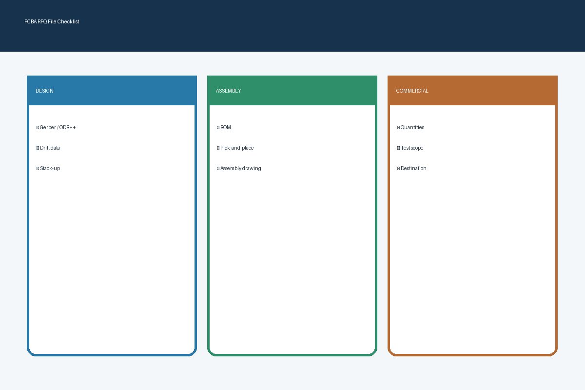
The PCB DFM report workflow can turn the proposed correction into explicit fabrication and assembly dispositions before the respin is released.
Review signal, return, and protection paths together
An ARINC 429 line-interface change can affect differential waveform shape, balance, source impedance, receiver margin, common-mode response, and conducted or radiated behavior. Review both conductors and the associated return and shield architecture. Do not route a patch wire by visual convenience across noisy power stages, clock regions, plane gaps, or protection-current paths.
Component pads, long branches, test points, and wire loops add parasitic inductance and capacitance. These effects may be unimportant for one slow control node but significant at a line driver, receiver input, fast digital interface, or transient-protection network. Compare the modified geometry with the original analysis and measurement bandwidth.
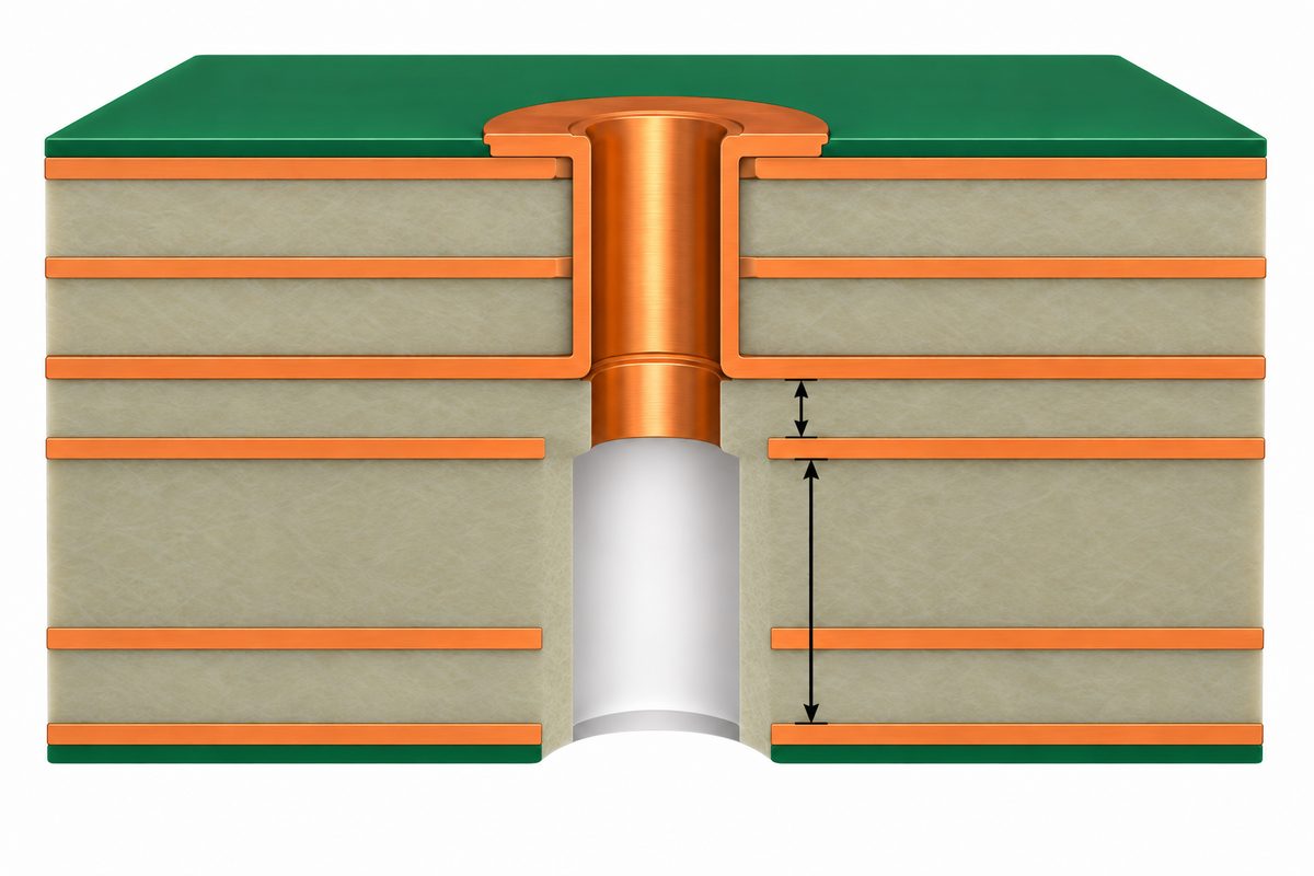
The high-speed PCB design guide explains how reference planes, return paths, vias, discontinuities, loss, and verification should remain connected to the production stackup.
Do not treat protection as an isolated component swap
Protection performance depends on the device, series elements, board layout, connector location, ground or chassis connection, parasitic path, spacing, and energy-handling network. A lower nominal clamp value does not prove better protection if it adds line capacitance, changes leakage, distorts the waveform, or routes transient current through sensitive circuitry.
Identify which external threats and equipment-level test categories apply. RTCA describes DO-160 as a collection of environmental and electromagnetic test procedures for airborne equipment; it does not certify a component or PCB by itself. The project authority defines the applicable revision, categories, levels, installation, and compliance plan.
If a patch changes a protection device, return connection, connector interface, shield bond, or physical spacing, reassess the affected transient, susceptibility, emissions, insulation, and safety evidence. Do not claim that an earlier equipment test automatically covers a materially different current path.
Check power, thermal, and component consequences
A transceiver or line-driver change can alter supply rails, startup state, enable logic, digital thresholds, output behavior, heat dissipation, fault response, and test modes. Compare normal and worst-case power, package thermal path, junction-temperature estimate, exposed-pad connection, local copper, and nearby temperature-sensitive components.
For any alternate device, compare the complete orderable part number, grade, package drawing, pinout, recommended circuit, absolute maximum ratings, operating specifications, lifecycle status, and manufacturer change notices. Review firmware, FPGA, register, label-filter, FIFO, interrupt, and built-in-test dependencies where the device includes protocol functions.
A physically compatible package can still need a respin if decoupling, exposed-pad, filter, routing, or protection recommendations differ. Keep engineering approval separate from purchasing availability.
Assess mechanical and environmental durability
A wire or lead added to an airborne assembly must survive the intended vibration, shock, temperature, humidity, altitude, and service environment for its approved scope. Review wire mass, unsupported span, solder-joint stress, adhesive compatibility, coating, abrasion, clearance, and proximity to sharp or hot features. Hand routing can vary between operators unless the instruction and fixtures control it.
Conformal coating or staking can improve mechanical support, but it may complicate inspection, rework, contamination control, and future failure analysis. Use approved materials and cure processes. Do not bury an unverified solder joint under adhesive simply to make the patch appear robust.
When the board is installed in a chassis, confirm connector loading, mounting points, shield contacts, fastener torque, cooling, and cable bend. Bench behavior outside the enclosure may not represent the qualified installation.
Define verification from the change impact
Start with bench checks that directly address the failure: continuity, shorts, supply rails, current, logic state, transmitted word behavior, receiver response, channel isolation, and waveform measurements under representative cable and load conditions. Define probes, bandwidth, grounding, fixtures, limits, operating conditions, and calibration.
Then assess regression coverage. Exercise unaffected channels and functions that share supplies, clocks, processors, connectors, or returns. Include startup, shutdown, fault, and built-in-test behavior where relevant. Verify software or programmable-logic configuration and record the exact versions.
Environmental or electromagnetic retest scope should follow a documented impact analysis and the program’s approval process. It may range from focused engineering tests to broader equipment-level regression. Only the responsible certification or compliance authority can approve the rationale; a contract manufacturer should not invent that decision.
Plan test access before the respin is fixed. The PCB test-point design guide explains how electrical suitability, return access, fixtures, and released test documentation must align.
Release a configuration manufacturing can reproduce
For a temporary patch, issue a controlled rework instruction with applicability, materials, tools, preparation, step sequence, workmanship, inspection, cleaning, coating, identification, test, rejection, and record requirements. Update the as-built configuration and unit history. Do not rely on a technician’s memory or an annotated photograph stored outside document control.
For a respin, update schematic, layout, fabrication data, stackup, BOM, approved alternates, placement file, assembly drawings, programming files, test procedures, mechanical documents, and change history together. Reconcile exported files so that the new copper revision cannot be paired with an old BOM or test program.
Use a pilot build to confirm assembly, inspection, programming, and functional-test assumptions. Preserve golden samples or controlled comparison data where appropriate, but do not treat one working board as the entire acceptance plan.
What should be sent for quotation?
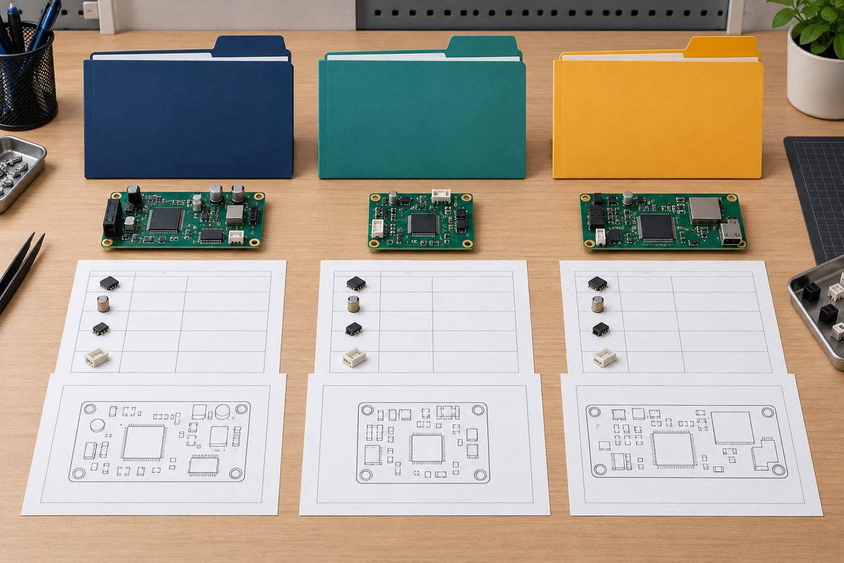
Provide the current and proposed schematic, PCB data, fabrication drawing, stackup, BOM, placement file, assembly drawings, patch or change description, affected net list, connector and cable information, software or FPGA versions, component data sheets, test requirements, inspection criteria, quantities, traceability, and approval constraints. Mark proprietary and controlled information according to the program’s procedures.
For a controlled prototype patch, send the exact instruction and verification plan through the PCB engineering quotation path. State that the configuration is for evaluation unless broader authority has already been documented.
For a respin and pilot build, use the PCBA RFQ page to define fabrication, component sourcing, assembly, coating or staking, programming, inspection, functional test, reporting, and delivery scope under one revision.
Patch-or-respin decision checklist
- Preserve the original failure evidence and exact equipment configuration.
- Define the modification and the question it is intended to answer.
- Trace affected electrical, mechanical, environmental, and compliance requirements.
- Review both ARINC line conductors, return paths, shielding, and protection.
- Compare exact components, packages, supplies, thermal behavior, and software dependencies.
- Assess wire routing, strain relief, coating, clearance, vibration, and inspection.
- Define bench, regression, and environmental retest scope through the approval process.
- Identify patched units and control their permitted use.
- Respin when the change cannot be made repeatable, inspectable, and durable.
- Release all fabrication, assembly, programming, and test documents together.
A patch should create evidence, not become an undocumented product architecture. For a one-stop review covering PCB fabrication, controlled component sourcing, assembly, rework, inspection, programming, functional testing, and pilot production, submit the approved data package through the AssyPCB RFQ page. The final authority for airborne compliance remains with the customer’s responsible engineering and certification organization.
Technical references: RTCA DO-160 overview, Holt Integrated Circuits ARINC 429 product resources, and Data Device Corporation data-bus component documentation.
Latest Blog

Contact Info
Phone: +86-755-82882936
Email: [email protected]
WhatsApp: +86-13570802455
Wechat: +86-13570802455
Address: 2nd floor,D Bldg.,Electric Link Technology Bldg.,Gongming,Guangming New Dist.,518106 Shenzhen, China