
IPC-7351 Footprints: Read Names and Verify Density Choices
Table of Conent
Table of Conent
An IPC-7351 footprint name describes a package family and selected dimensional fields; it does not contain every copper-pad dimension or establish that a footprint suits your assembly process. Read the name with its documented naming convention, then check the exact component drawing, land geometry, density goal, and released manufacturing outputs. For many surface-mount families, the final M, N, or L identifies a Most, Nominal, or Least material variant. These density choices are separate from IPC product Classes 1, 2, and 3.
For an OEM designer or assembly buyer, the useful decision is whether a particular footprint revision can be released for a specified part and build process. A familiar library name is only the starting point. The review below connects legacy IPC-7351 naming to current source documents, a real manufacturer example, and the stencil and placement files that manufacturing actually uses. It does not reproduce the licensed land-pattern calculation tables.
Check the standard basis before changing a library
Identify the library’s actual design basis before calling it current, obsolete, or suitable for migration. A new guideline is a reason to review assumptions, not permission to regenerate released boards silently.
The official IPC revision table, checked October 23, 2026, lists IPC-7351B from June 2010 as no longer maintained and separately lists IPC-7352. The public IPC-7352 sample carries a May 2023 date, while the revision table lists its original issue as July 2023. Record the source being used rather than asserting that those dates are identical.
The IPC-7352 public scope addresses land patterns for surface-mount and through-hole components and allows documented adjustments for company or board technology needs. This article uses its public scope only; the complete calculation tables were not reviewed. Do not interpret a generic guideline as validation of every company-specific footprint.
Keep the footprint’s source revision, generator settings, approved modifications, and intended process with the library record. If an established product was released using a legacy basis, decide deliberately whether to retain it or qualify a changed geometry. A naming cleanup and a physical land-pattern change need different review scopes.
Read the name as a descriptor, not a pad drawing
Decode fields according to the package family and the library’s documented convention. A number in the name may describe the component outline rather than the copper geometry on the board.
NI’s Ultiboard documentation, updated May 8, 2026, explains that IPC-7351B names carry package type, pitch, span, body dimensions, and pin quantity. It also states that its IPC-compliant patterns use nominal density. That is a specific library implementation, not evidence that every downloaded footprint uses the same default.
The PCB Libraries naming guide gives the SOIC grammar as family, pitch, nominal lead span, height, and pin quantity, with a density suffix. For this family, 127P represents 1.27 mm pitch and a span field of 600 represents 6.00 mm. Neither value specifies pad length. Other families use different fields; do not apply this grammar blindly to a BGA or a package with omitted terminals.
Names can also collide: the guide notes that different manufacturer tolerances can produce different pads or courtyards under the same footprint name. Preserve a unique internal identifier and revision. The broader component-library verification workflow addresses part identity and pin mapping; this review focuses on the geometric meaning and limits of the name.
Choose a density goal with the assembly process
Select a density goal from the actual component and manufacturing constraints. “Least material” should not be chosen merely because the board is crowded, and “Most material” is not a higher reliability class.
| Suffix and level | Meaning | Decision to review | What remains unproven |
|---|---|---|---|
| M / A | Most material | Can the resulting geometry coexist with adjacent parts and process needs? | Actual spacing, paste behavior, and product reliability |
| N / B | Nominal material | Does the nominal configuration match the intended part and process? | Compatibility with a particular manufacturer’s tolerances |
| L / C | Least material | Has the proposed geometry been reviewed for the intended assembly conditions? | A production-capable result merely from the suffix |
These meanings follow the cited PCB Libraries guide. Its BGA treatment is an exception to the simple three-variant description. Keep density labels distinct from the end-use classifications discussed in the assembly acceptance-class guide. Renaming N to M does not change the physical pads, and assigning Class 3 does not select a density suffix.
A useful proposed comparison records the selected variant, component drawing, copper geometry, surrounding placement, and manufacturing assumptions together. Ask the assembler to identify unresolved process constraints before buying parts or releasing tooling. Avoid choosing a variant from a generic rule about board size or product category.
If the density choice remains open, share the exact part numbers and proposed footprint views with the package drawings, available placement space, build quantity, and process questions so manufacturing assumptions can be reviewed before the stencil and sourcing decisions are fixed.
Verify a named pattern against the actual manufacturer drawing
Compare separately published package and land-pattern dimensions before drawing conclusions from a filename. A manufacturer example makes the distinction between lead span and copper-pad spacing measurable.
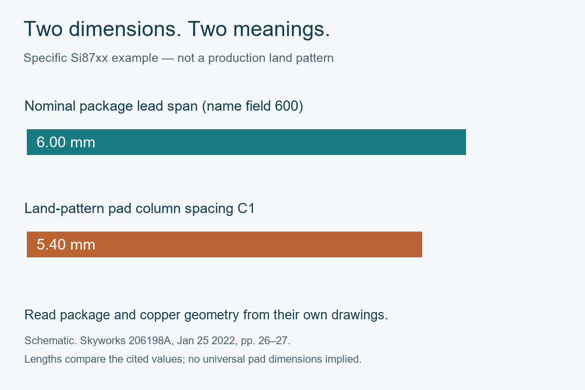
The Skyworks Si87xx data sheet, document 206198A dated January 25, 2022, references SOIC127P600X173-8N for its narrow-body SOIC land pattern. Pages 26–27 provide the package outline and recommended lands separately. The following values belong to that cited example, not to every SOIC-8.
| Item | Cited value | Review implication |
|---|---|---|
| 127P pitch field | 1.27 mm; package e and land-pattern E | Check the physical terminal pitch and CAD pad pitch |
| 600 nominal lead-span field | 6.00 mm; package H ranges from 5.80 to 6.20 mm | Do not use this as pad-column spacing |
| Pad-column spacing C1 | 5.40 mm | Read the land-pattern drawing separately |
| Pad width X1 and length Y1 | 0.60 mm and 1.55 mm | These copper dimensions are not encoded by the span field |
| Height descriptor X173 | 1.73 mm in the name; package A is separately listed as 1.35–1.75 mm | Keep the name and outline evidence distinct; clarify the basis if it affects the design |
The land-pattern notes identify Density Level B and assume a 0.05 mm card fabrication tolerance. Preserve those conditions with the example. Do not “correct” a published name or copy these pads to another part without resolving its source and process basis.
For a mechanical clearance check, use the applicable package-outline limit and the project’s clearance rules rather than treating the height-coded name as a guaranteed maximum. The different height values alone do not prove that the published copper geometry is wrong.
Carry geometry changes into stencil and placement outputs
When copper geometry changes, review the manufacturing artifacts derived from it. A revised CAD library does not establish that the exported board, stencil, and placement data were regenerated consistently.
Use a proposed change-impact record to distinguish three cases. An identity-only rename needs confirmation that the released geometry and mapping remain unchanged. A pad or courtyard change needs a physical comparison and review of affected board clearances. A process-specific adjustment needs the responsible owner to document what was changed and why, with the appropriate manufacturing review.
Keep copper and paste as separate outputs. The IPC-7352 public introduction identifies mask, stencil apertures, adjacent-component clearance, and process conditions as considerations beyond the basic land geometry. It also states that heat dissipation and shock/vibration effects are outside the guideline’s consideration. A familiar density code therefore cannot close an application-specific thermal or mechanical question.
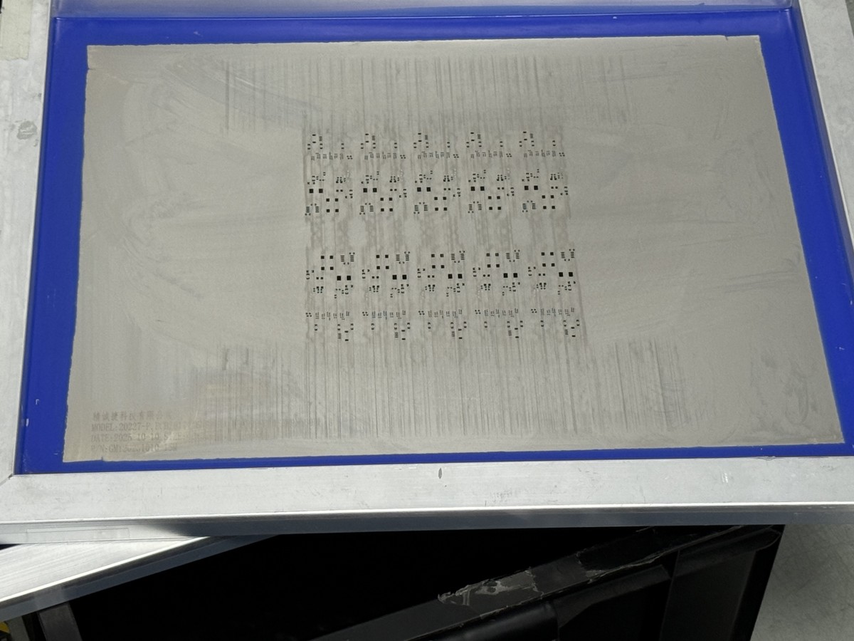
For the affected references, compare exported copper, mask, paste, pad numbering, origin, rotation, and board side. Keep any placement-convention translation explicit. Retain the earlier released files for traceability rather than overwriting them with a new library export that has the same filename. Record which artifact revisions were reviewed together.
Release a footprint by revision and intended use
Release the verified geometry and its intended use, not just the name. The receiving manufacturing team needs enough information to reproduce the chosen configuration without selecting a different library variant by guesswork.
Identify the exact manufacturer part, package drawing revision, internal footprint identifier and revision, naming convention, density basis, and approved exceptions. For alternates, verify each orderable part against the selected geometry; a shared family label does not authorize substitution. Preserve the evidence for a legacy footprint when it remains the approved choice.
A turnkey PCB assembly scope can coordinate board fabrication, component sourcing, and assembly, but the customer’s released design basis still needs to be unambiguous. Resolve whether an engineering question is open before treating a quotation as permission to alter the footprint.
The name is useful for finding and discussing a pattern; its verified geometry, source conditions, and revision support the build decision. When the design is ready, provide the released fabrication, BOM, and placement package with assembly drawings, footprint exceptions, quantities, and test requirements so the complete project can receive a coordinated engineering and quotation review.
Source review: October 23, 2026. Numerical values are a bounded manufacturer example. The change-impact workflow is a recommendation, not additional IPC requirements.
Latest Blog
Contact Info
Phone: +86-755-82882936
Email: [email protected]
WhatsApp: +86-13570802455
Wechat: +86-13570802455
Address: 2nd floor,D Bldg.,Electric Link Technology Bldg.,Gongming,Guangming New Dist.,518106 Shenzhen, China