
Automated Optical Inspection (AOI) in PCB Assembly
Table of Conent
Table of Conent
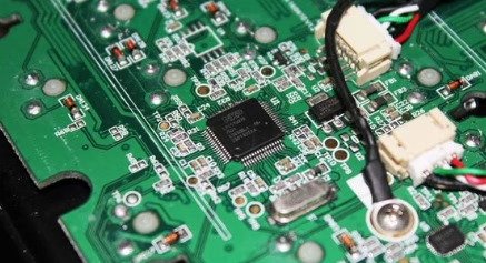
Automated optical inspection (AOI) uses cameras, controlled lighting, and image analysis to flag visible defects on a bare PCB or assembled PCBA. In assembly, it is most useful for finding missing or misoriented components, placement errors, solder bridges, and other visible solder-joint anomalies before a board moves to later tests. AOI is an inspection method, not an electrical or functional test: hidden BGA joints, internal voids, and circuit behavior need other methods. For a reliable build, specify which defects matter, where AOI sits in the process, how flagged boards are reviewed, and what additional testing the design requires.
What does AOI inspect in PCB assembly?
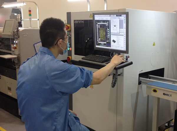
AOI compares captured board images with an approved reference, CAD-informed program, or programmed feature rules. The system highlights differences for an operator or quality engineer to review. The result depends on lighting, camera angle, component geometry, program setup, and the acceptance criteria selected for the build. A flagged area is a finding to verify, not automatic proof that the board has failed.
For bare boards, optical inspection can examine visible copper and surface features. For assembled boards, it checks the visible placement and soldering result. These are related uses, but they should not be confused with solder paste inspection (SPI) before placement or with electrical continuity testing after assembly.
Why use AOI alongside manual inspection?
Repeatable imaging helps teams inspect many similar features consistently and retain evidence of detected anomalies. It can also reveal process trends: repeated bridges on one footprint, polarity findings on one variant, or a change in placement offset may point to a stencil, program, feeder, or reflow issue. Manual review remains important for confirming false calls, judging ambiguous joints, and deciding the appropriate rework or process response.
For high-mix, low-volume work, the decision is less about maximum line speed and more about setup discipline. Each board revision or variant needs the correct program, reference, BOM, polarity map, and first-article review. A short run with the wrong program can create more uncertainty than a carefully planned combination of AOI and targeted manual inspection.
How does an AOI test work?
1. Capture and illuminate the board
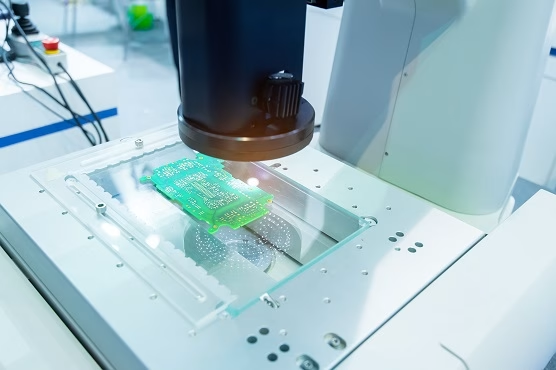
Cameras image the target features under controlled illumination. Different angles and colors improve contrast on component bodies, polarity markings, leads, and visible solder fillets. Some systems measure height or shape with 3D techniques, but the available measurement and defect coverage depend on the particular machine and program.
2. Compare features with the approved build
The software compares images or measured features with an approved reference and programmed tolerances. CAD, placement, and BOM data can support program creation, but Gerber files alone do not define every mounted component, polarity rule, or acceptable solder joint. The production team must control the correct data set for each revision.
3. Verify calls and record disposition
An operator reviews suspected defects and separates real findings from false calls. Confirmed defects are recorded, repaired or segregated according to the agreed process, then reinspected when appropriate. Trend reports are valuable only if the program and review decisions are controlled; a raw count of flagged images is not a yield metric.
Which defects can AOI find, and which can it miss?
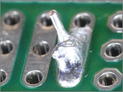
AOI is well suited to visually accessible defects: missing or shifted parts, some polarity mistakes, lifted leads, visible bridges, insufficient-looking solder, solder balls, and surface damage. Whether it catches a specific condition depends on the package, camera view, lighting, and criteria. A printed component value may be read only when markings are visible and the program is configured for it; AOI cannot prove an unmarked component’s electrical value or authenticity.
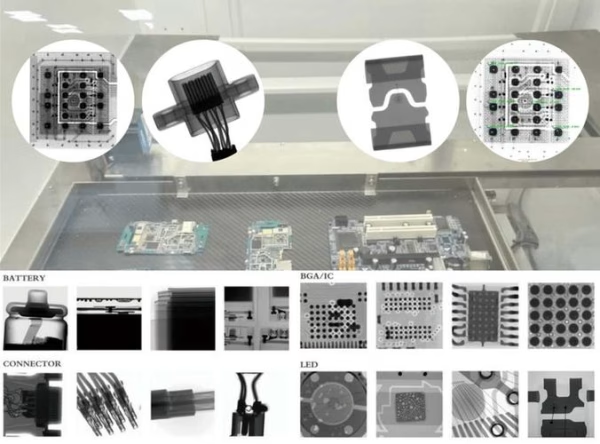
AOI cannot see through an opaque package. It does not directly establish electrical continuity, insulation, firmware behavior, or performance under operating conditions. Hidden solder joints and internal voids may require X-ray inspection with defined acceptance rules; electrical or functional tests answer different questions. This visibility boundary is the key reason not to describe AOI as a complete test of every board.
Where should AOI be placed in the manufacturing flow?
Before component placement, solder paste inspection can measure deposited paste and help correct printing problems before they become assembly defects. Pre-reflow AOI checks placed components before soldering; post-reflow AOI examines the assembled result, including visible solder joints. The right combination depends on board complexity, package visibility, volume, and the cost of finding a defect late. In an automated PCB assembly workflow, revision control, setup verification, AOI review and the agreed test plan should be coordinated rather than treated as isolated machine steps.
AOI systems may be in-line or off-line, use top-down and angled views, and analyze 2D images or 3D surface information. These configurations are not interchangeable promises of coverage. For instance, a 3D optical view can improve assessment of visible shape or height but still cannot inspect solder hidden beneath an opaque BGA body. Ask for the actual inspection point and target defects, not only the machine label.
How does AOI compare with X-ray, ICT, flying probe, and functional test?
Choose the method from the failure mode that must be detected. The methods complement one another; no single inspection step establishes all aspects of board quality. The table below is a planning guide, not a promise that every method is available or suitable for every design.
| Method | Strongest use | Important limit | When to specify it |
|---|---|---|---|
| SPI | Solder paste deposits before placement | Does not assess completed joints or function | Fine-pitch printing risk or paste-process control |
| AOI | Visible placement and solder anomalies | Cannot see hidden joints or prove electrical behavior | Visible assembly defects and process feedback |
| AXI / X-ray | Hidden joints and certain internal solder conditions | Needs image interpretation and agreed criteria | BGA, QFN, or other obscured-joint risk |
| ICT / flying probe | Selected electrical nets, component values, or assembly faults | Coverage depends on access, fixture, program, and design | Electrical fault isolation where test access is available |
| Functional test | Specified board behavior under defined conditions | May not identify the physical root cause | Release requirements tied to real product operation |
For more detail on electrical access and setup economics, see the site’s flying-probe versus bed-of-nails comparison. IPC describes IPC-A-610J as a post-assembly acceptance standard; the required class and any customer-specific criteria should be agreed for the project. OMRON documents the visibility limitation of optical inspection for hidden solder.
If your assembly has inaccessible joints or defined electrical release criteria, share the board files, BOM, quantity, and required inspection evidence so the complete fabrication, sourcing, assembly, and test scope can be reviewed together.
What changes for high-mix, low-volume PCB assembly?
Frequent changeovers make revision control and material traceability especially important. The first article for each variant should match its own BOM, placement file, polarity instructions, and AOI program. A useful handoff identifies which defects trigger hold or rework, whether X-ray or electrical testing is needed, and what record the buyer expects with shipment. This avoids treating every variant as if it had the same inspection coverage.
OrinewPCB’s one-stop PCB assembly service coordinates PCB fabrication, component sourcing, assembly, and testing for prototypes and small batches with multiple variants. The company states that sourced materials are 100% brand-new original components and uses a nine-step quality workflow; the exact inspection and test activities for a board should be confirmed in the build plan. Cooperation with manufacturers and distributors can support competitive material pricing and availability, while the final quote and fastest practical delivery depend on the approved BOM, quantities, and required tests. The turnkey assembly service explains the wider handoff.
What determines AOI cost and lead time?
For a buyer, the meaningful cost is the inspection scope within the total assembly quote, not an unsupported purchase price for an AOI machine. Programming a new board or revision, first-article verification, panel design, board complexity, inspection points, false-call review, rework, reporting, and any supplementary X-ray or electrical tests all affect effort. Component lead time and fabrication requirements may dominate the delivery schedule even when AOI itself is quick.
To get a useful comparison between suppliers, ask what is inspected, at which stage, against which acceptance criteria, how suspect boards are dispositioned, and what evidence is delivered. A low quoted inspection cost can be misleading if hidden-joint or functional requirements were omitted.
What should a buyer include in an AOI and PCBA RFQ?
Provide the released Gerber or ODB++ package, BOM with approved manufacturer part numbers and substitution rules, centroid or pick-and-place file, assembly drawings, board revisions, quantities by variant, target schedule, and any inspection or electrical test requirements. Call out BGAs, QFNs, fine-pitch parts, polarity-critical devices, traceability requirements, and the acceptance standard or customer criteria you expect. This lets the team assess AOI coverage and decide where another test is needed before promising a delivery date.
Practical next step: If you need one team to coordinate boards, 100% new original components, assembly, and a defined inspection plan, send the released build package and test requirements for a combined review. OrinewPCB can then confirm material availability, inspection coverage, lead time, and a project-specific price.
AOI inspection: the decision in brief
AOI makes visible PCB assembly defects easier to detect consistently, but it cannot replace X-ray for hidden solder or electrical and functional testing for circuit behavior. A sound quality plan ties each inspection method to a failure mode, controlled reference, acceptance criterion, and disposition rule. For high-mix, low-volume builds, revision and program control matter as much as the machine specification.
Latest Blog



Contact Info
Phone: +86-755-82882936
Email: [email protected]
WhatsApp: +86-13570802455
Wechat: +86-13570802455
Address: 2nd floor,D Bldg.,Electric Link Technology Bldg.,Gongming,Guangming New Dist.,518106 Shenzhen, China