
EV BMS PCB Design: Release the Sense Map and Isolation Boundaries
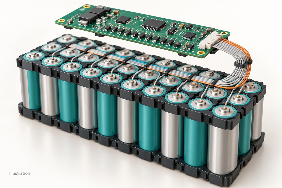
Table of Conent
Table of Conent
EV BMS PCB design is ready for manufacturing when the cell-sense map, electrical domains, balancing conditions, and acceptance tests describe one controlled configuration. The battery management system must associate each reported measurement with the correct physical cell boundary. A plausible voltage reading alone does not prove that identity. Release the connector-to-channel map and insulation-boundary drawing alongside fabrication, assembly, firmware, and test files before ordering a pilot build.
This guide addresses OEM hardware engineers and PCBA sourcing and test teams preparing a cell-monitoring board for production. It does not specify a complete traction battery or a universal insulation distance. The approved battery architecture, selected monitor, operating environment, and safety requirements control those decisions. The useful manufacturing outcome is a board whose identity, build variant, and measured behavior can be traced back to those requirements.
Make the sense map authoritative
The sense map should connect physical cell boundaries to connector cavities, PCB nets, analog front-end inputs, and software channel indices. Treat that map as a released engineering document. A schematic net label and a firmware array index can both look correct while referring to different physical cells.
A cell channel normally represents a difference between two sense-node potentials. The selected monitor determines which inputs, filtering, unused-channel connections, and diagnostic modes are permitted. The current TI BQ7961x-Q1 data sheet, for example, gives device-specific cell-input and unused-pin connections and describes open-wire checks that depend on ADC configuration, thresholds, and settling. Apply the exact part and revision rather than transferring those settings to another monitor family.
| Mapping boundary | Required record | Question resolved |
|---|---|---|
| Physical cell or busbar | Module identity, adjacent node names, polarity | What voltage difference should this channel represent? |
| Harness and connector | Cavity numbers, mating-view drawing, harness revision | Which physical contacts carry those nodes? |
| PCB and monitor | Net names, filter references, exact input pins | Does the assembled path match the approved circuit? |
| Firmware and test | Register/channel index, variant, stimulus and expected result | Does the reported channel identify the intended cell? |
Include busbar channels, unused positions, temperature inputs, and board variants where applicable. Distinguish a deliberately unused channel from a disconnected required wire. Identify connector orientation by the actual mating view; a drawing viewed from the wire side can reverse the apparent cavity order.
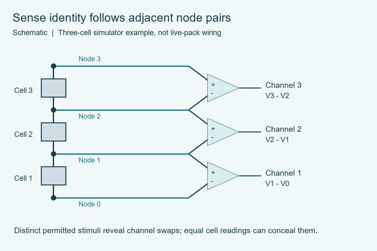
Give the map a revision and an approval owner. Changes to a harness, connector, filter population, monitor, or software mapping should trigger an impact review even if the bare-board outline does not change. Production needs the final relationship, not separate documents that each require an operator to infer the missing link.
A mapping review should also identify the reference used by the test station. If the station wiring and the firmware table were generated from the same incorrect spreadsheet, agreement between them is weak independent evidence. Compare both against the released connector and cell-boundary drawing. Document the direction of channel numbering, reserved positions, and any busbar exception explicitly. Keep simulator output names separate from device register names so a technician can trace the physical connection without assuming that matching numbers imply matching signals.
Release isolation boundaries by electrical domain
An isolation boundary belongs between named electrical domains under defined operating and transient conditions. Do not assign every local PCB spacing from the pack nameplate voltage, or assume a floating monitor circuit has the same reference as the vehicle controller.
Draw the cell-stack reference, local monitor supply and return, communication connection, isolated power if used, chassis or shield connections, and the low-voltage host domain. Identify every intended crossing: communication components, power converters, protection, connectors, mounting hardware, and test access. State the voltage relationship and insulation function required for each pair of domains.
TI’s creepage and clearance training explains that spacing depends on working voltage, materials, environment, and the applicable requirements. Analog Devices likewise distinguishes working voltage from isolation test voltage. A component withstand rating is therefore an input to the design review, not a complete PCB spacing rule.
Translate the approved boundary into fabrication and assembly constraints: copper and component keepouts, slots where specified, material requirements, connector geometry, contamination controls, and inspection access. Preserve the limits through tooling and handling. A fixture connection or mounting feature can cross a boundary that looked clear in the layout.
The functional-safety evidence boundary explains why a capable component and acceptable workmanship do not establish system-level safety performance. The OEM remains responsible for the product’s safety requirements and validation plan; manufacturing executes the agreed controlled build and tests.
Once these boundaries and variants are defined, send the sense map and controlled board files with the BOM and insulation constraints so the manufacturing review can align layout restrictions, assembly access, and acceptance responsibilities before the pilot.
Control balancing heat and measurement conditions
Balancing is a thermal and measurement condition that belongs in the release package. Define the permitted channel combinations, duty cycle or operating mode, temperature monitoring, and measurement state from the actual design. A resistor rating alone does not establish acceptable board temperature.
The ADI battery-stack monitor discussion describes the energy dissipation and thermal tradeoff of passive balancing. For a production review, identify where that heat goes and which nearby references, filters, sensors, connectors, or insulating materials it can affect. Consider the intended enclosure and cooling arrangement when defining the representative validation setup.
Specify resistor values, ratings, package and approved alternatives; switching-device and monitor restrictions; copper construction; and any thermal interface or spacing requirements. A substitution that preserves resistance can still change heat distribution or assembly access. Require engineering approval when those characteristics matter.
Separate measurement conditions in the test procedure. Record whether balancing is disabled, enabled on selected channels, or operating in a defined sequence. Include the settling and sampling conditions needed for the chosen monitor. Compare results against the same declared state rather than treating every difference as a soldering defect.
Cleanliness and laminate reliability also require deliberate controls around biased circuitry. The official OrinewPCB explanatory video below discusses conductive anodic filament formation inside laminate. It is labeled as AI-generated educational content, not footage of a BMS product or a measured factory failure.
Use the approved material, process and environmental evidence to select controls. Do not assume coating, a clean appearance, or a passed initial electrical test proves long-term insulation reliability.
Test channel identity before accepting measurement accuracy
Prove that each reported channel corresponds to the intended physical input before evaluating its accuracy. Equal simulated cell voltages can hide a permutation: the numbers still look plausible after channels are swapped. Use a validated, controlled cell simulator and a distinguishable stimulus pattern within the approved board limits.
TI’s BMS hardware-emulation discussion provides context for controlled development stimuli. For production, define the actual simulator, connection sequence, protection, common-mode capability, fixture checks, and expected responses. Do not use uncontrolled live-pack disconnections as a substitute for a released fault-test method.
| Decision | Evidence | Release consequence |
|---|---|---|
| Channel identity | Distinct valid stimulus per mapped input and matching reported index | Resolve mapping errors before accuracy acceptance |
| Measurement performance | Specified points, uncertainty, state and settling conditions | Compare against approved limits, not display resolution |
| Open-wire diagnostic | Approved simulated fault with correct configuration and completion status | Record detection coverage and excluded cases |
| Balancing interaction | Declared channel combination and thermal/measurement state | Accept only under the specified operating conditions |
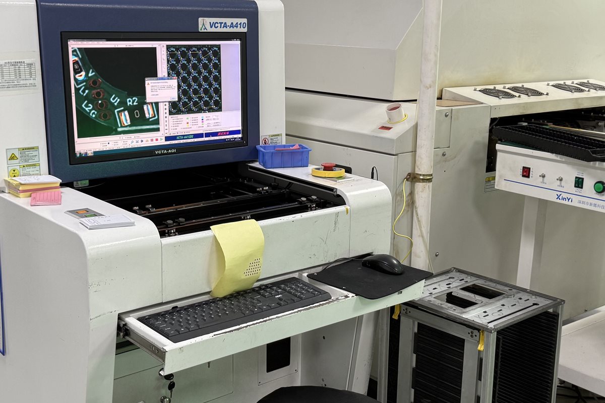
Use a requirement-to-test record to connect each test to its purpose, stimulus, observation, limit, and retained result. Validate the station with approved known conditions so a cable or configuration error is distinguishable from a failed board. Preserve raw results where needed for investigation.
Distinguish an engineering characterization from the recurring production screen. Characterization can establish the behavior across the specified operating range and enclosure conditions; the production screen checks agreed features under a repeatable station setup. Record why the selected production points cover the intended assembly faults and what remains dependent on design validation. When a test limit or station setting changes, review that coverage rather than simply updating the pass/fail file.
Close the pilot with reproducible channel evidence
Release the pilot only when hardware identity, programmed configuration, mapped measurements, and acceptance records agree. A passing summary without fixture or software identity cannot support a useful comparison after a change.
The full-turnkey PCB assembly scope supplies the broader sourcing and manufacturing framework. Add the BMS-specific map, domain drawing, balancing constraints, approved device documentation, and test ownership. State who supplies the simulator and who maintains the test procedure.
Retain board revision, BOM and approved alternates, firmware/configuration identity, harness and fixture revision, inspection results, channel test results, deviations, and retest dispositions at the agreed lot or serial level. Define change effectivity so a corrected mapping cannot silently enter only part of a lot.
An EV BMS PCB release should make every measurement and boundary traceable to an approved design decision. When that package is ready, provide the complete BMS assembly package with Gerber or ODB++ files, BOM, placement data, quantities, and acceptance requirements to align fabrication, sourcing, assembly, and test preparation for the build.
Latest Blog


Contact Info
Phone: +86-755-82882936
Email: [email protected]
WhatsApp: +86-13570802455
Wechat: +86-13570802455
Address: 2nd floor,D Bldg.,Electric Link Technology Bldg.,Gongming,Guangming New Dist.,518106 Shenzhen, China