
Drilling-Rig Instrumentation PCBs: When HDI and Microvias Are Justified

Table of Conent
Table of Conent
A drilling-rig instrumentation PCB needs HDI only when the actual component pitch, routing density, board outline, or layer-transition plan cannot be met with a simpler qualified construction. A hazardous-area designation is a separate equipment and circuit assessment; it does not automatically call for microvias. Start with the instrument’s installation and protection concept, identify the circuits and package escapes that set the layout, and then choose the least complex via structure that both the fabricator and the assessment owner can verify. A single blind microvia may solve a fine-pitch escape without the added interfaces of a stacked structure. The purchase package must preserve the approved spacing geometry, exact stackup, fabrication evidence, assembly heat exposure, and change-control rules.
Decide whether HDI is necessary for the instrument
HDI should answer a demonstrated routing constraint, not a general statement that a drilling rig is harsh. Place the selected sensor interface, processor, connectors, protection components, mounting features, and keep-out areas on the real board outline. Route the critical nets with conventional plated through-holes first. If a fine-pitch package traps escape routes or through-holes consume required routing channels, compare a one-level blind-microvia build against a larger outline, a different package, or another layer arrangement. The BGA escape and HDI release guide explains why the package transition should drive this choice.
The term “instrumentation” covers very different assemblies: a sensor interface near a hazardous process, an associated control unit elsewhere, and a protected enclosure may have different electrical and mechanical boundaries. The equipment owner must supply the actual installation, connection and protection requirements. Neither a rig setting nor a compact board alone proves that the whole instrument is intrinsically safe.
The HDI PCB manufacturing overview can frame an initial fabrication discussion, but it cannot replace a review of this instrument’s specific via stack, safety-related artwork and acceptance plan.
| Observed design condition | First layout option to examine | Release decision |
|---|---|---|
| Connector, discrete and processor routes escape without congestion | Conventional multilayer board with qualified through-holes | Keep the simpler construction unless outline or performance constraints justify more complexity. |
| One fine-pitch package blocks outer-layer escape | One blind microvia level into the next layer | Request the exact dielectric, target-pad, drill and plating capability before freezing the stackup. |
| Routing study still needs multiple build-up transitions | Compare staggered or stacked microvias with the fabricator | Document why the added transitions are necessary and how coupons and assembly preconditioning will be accepted. |
That table is a routing decision, not a generic design-rule minimum. The chosen fabricator’s documented process and the equipment owner’s approved design control the actual dimensions.
Keep intrinsic-safety assessment separate from the HDI label
Intrinsic safety concerns whether the assessed electrical apparatus and its circuits can ignite a surrounding explosive atmosphere under the applicable conditions; the PCB fabrication class alone cannot establish it. IEC 60079-11:2023, including the IEC’s current corrected version, describes construction and testing of intrinsically safe apparatus and associated apparatus. It does not make every drilling-rig board an intrinsically safe board. The protection concept, hazardous-area classification, connected equipment, fault assumptions and applicable edition need to be set by the system owner and assessment body before the layout is released.
NSW TestSafe’s assessment description says schematics, interconnections and PCB layouts are examined, with critical board spacings measured from Gerber data. A PTB documentation checklist likewise calls for board drawings that show safety-determining parts and separations. Those are examples of assessment evidence, not permission to copy a distance from a web article. If a safety-related boundary runs through a dense region, have the assessor review the actual layer artwork, conductor geometry, barriers, coatings where credited, and controlled manufacturing tolerances. Reducing a spacing merely to fit a microvia fan-out could change the assessed circuit.
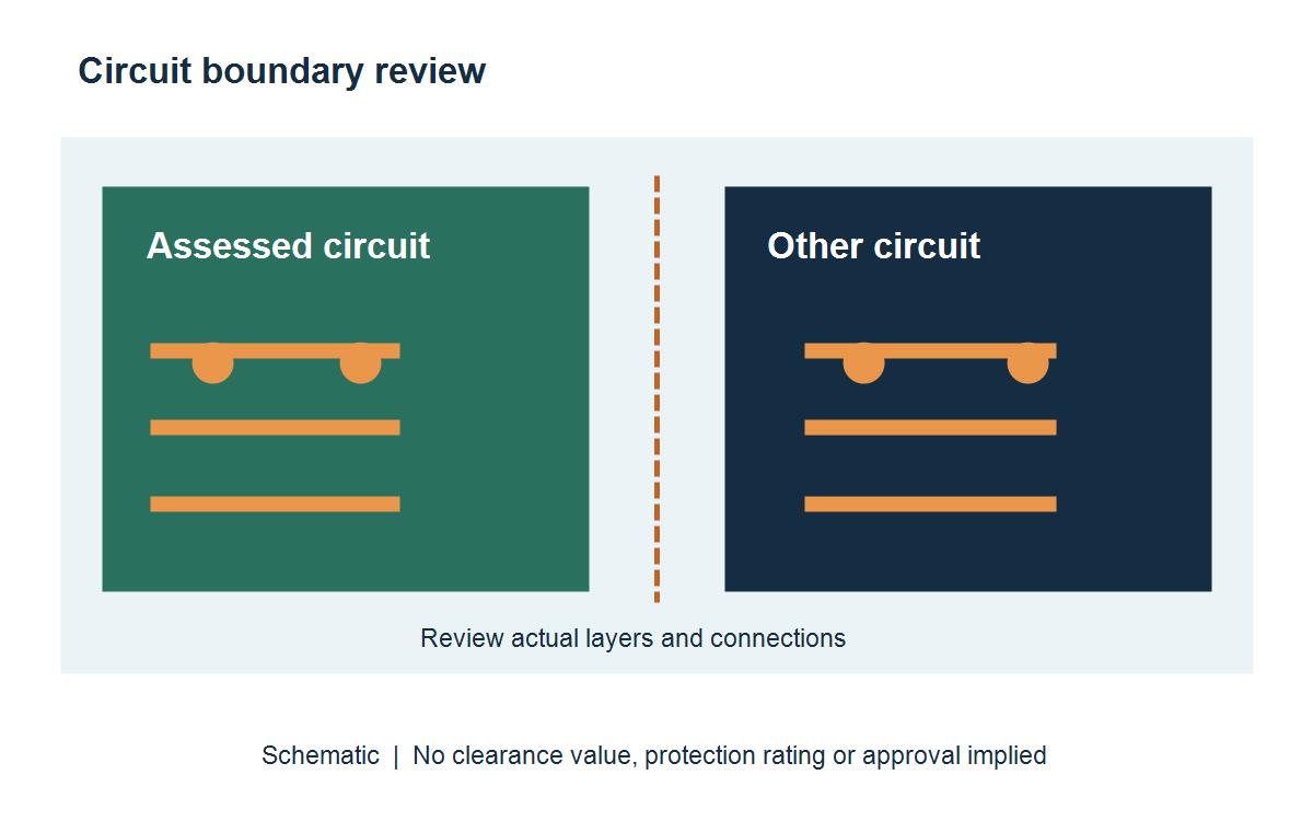
The related intrinsically safe telemetry PCBA handoff covers configuration ownership. This article addresses a narrower question: when HDI is justified and how the resulting via construction enters that controlled assessment.
Release a microvia structure that can be evaluated
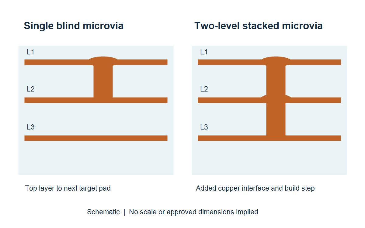
A microvia drawing must identify what each laser-formed connection reaches, not simply say “HDI.” Mark the start and target layers, finished land geometry, dielectric, fill/cap requirements where applicable, registration, and whether successive microvias are staggered or stacked. A stacked arrangement adds an interface over a lower via. It may be necessary for routing, but it should carry explicit build and acceptance evidence rather than an assumption that more density means more reliability.
IPC’s microvia reliability warning reports latent weak-interface failures that can appear after reflow even when room-temperature checks look acceptable. This does not say every microvia fails. IPC’s IPC-6012F release highlights expanded microvia-structure requirements and test coupons for complex interconnections. Treat the applicable standard revision, product class, coupon design and pass criteria as explicit purchase-order items agreed with the fabricator and OEM.
| Via topology | Useful when | Evidence to request before approval |
|---|---|---|
| Conventional plated through-hole | Routing and usable board area permit full-depth drilling | Released stackup, hole-to-copper geometry, plating acceptance and thermal exposure. |
| Single blind microvia | One outer-layer package escape needs a short transition | Target-layer drawing, laser/drill geometry, pad registration, plating/fill process and representative coupon. |
| Staggered or stacked build-up | Documented routing cannot be solved with one transition | Every interface and lamination cycle, approved process sequence, representative coupon, reflow preconditioning and agreed continuity/section criteria. |
If the selected escape strategy is still uncertain, share the stackup, BGA escape and via-coupon requirements for review with the board outline, assembly temperature profile and intended build quantity. The resulting scope can then identify which construction is feasible to quote and what evidence remains the OEM’s responsibility.
Qualify the build and assembly heat path together
A fabricator’s bare-board acceptance is not the end of the microvia decision. Reflow, any selective-solder operation, approved rework, and later thermal exposure add a history to the actual interconnect. Request representative coupons and a test sequence aligned to the assembled product rather than accepting a bare-board room-temperature continuity result as the sole proof. The appropriate criterion depends on the adopted specification, via structure and program risk. Do not translate IPC’s warning into a universal temperature or cycle count.
Release the exact laminate and build-up material, core/prepreg stack, target-pad interfaces, finish, via fill/cap route where used, and controlled substitutions. The PCB lamination guide provides context for why lamination sequence affects a multilayer build. The board shop should state what its process has been qualified to manufacture; the OEM should approve the structure and acceptance plan; the assembler should record the thermal profile and any rework applied to the accepted lot. If the instrument also needs environmental testing, select exposures from the actual installation and failure mechanisms, as discussed in the environmental test selection guide.
For example, a sensor module mounted near vibrating machinery and a control board in a conditioned cabinet should not inherit the same test plan merely because both belong to one rig. Record where each assembly is installed, the enclosure and connector interfaces, the expected service range supplied by the equipment owner, and any cleaning, moisture or mechanical stresses that the program actually specifies. Then ask which failure mode each proposed test is intended to reveal. The answer may change the fixture, coating or connector choice without changing the via topology. Conversely, a reliable package escape still needs a separate review of any protection-related circuit boundary.
Assign the evidence before a purchase order
The purchase order should connect every safety-relevant drawing and every microvia acceptance record to an accountable owner. A dense PCB can pass ordinary fabrication inspection and still be unusable if the reviewed circuit boundary changed, a build-up material was substituted, or an assembly rework history was lost. Specify what may change, who approves a change, and which records must follow the serial or lot number.
| Decision or record | Primary owner | Release/acceptance question |
|---|---|---|
| Hazardous-area/protection concept and circuit assessment | Equipment OEM and responsible assessment body | Which circuits, separations, faults and connected equipment are within the approved scope? |
| Layer artwork, netlist, package escape and safety boundary | OEM design authority | Do actual Gerber/ODB++ layers and controlled drawings match the reviewed design? |
| Microvia build sequence, material and representative coupons | Board fabricator with OEM acceptance | Does the exact topology survive the agreed preconditioning and inspection criteria? |
| BOM, assembly profile, rework and test configuration | EMS/assembler with OEM release | Are substitutions and thermal history traceable to the accepted board and equipment configuration? |
These rows are a handoff framework, not a certification checklist. They help the buyer avoid asking a board supplier to approve an equipment-level protection concept or treating an assembler’s visual inspection as proof of microvia endurance.
Send one controlled package through fabrication and assembly
Freeze the routing need, via topology and intrinsic-safety review boundary before the pilot build. A useful release includes the approved layer stack, Gerber or ODB++ data and drill files, controlled safety-relevant layout notes, BOM and alternates, pick-and-place data, assembly drawing, expected thermal process, test/coupon plan, build quantity, and owner for each exception. Where certification or hazardous-area assessment is required, keep the responsible assessor in the change loop; a PCB or PCBA quote does not confer equipment approval.
The practical decision is to use the simplest construction that solves the instrument’s real routing problem while retaining the approved circuit geometry and a verifiable thermal and test history. For a ready project, send the released board and assembly package together so fabrication, sourcing, assembly, testing and quotation assumptions can be checked against the same configuration.
Latest Blog

Contact Info
Phone: +86-755-82882936
Email: [email protected]
WhatsApp: +86-13570802455
Wechat: +86-13570802455
Address: 2nd floor,D Bldg.,Electric Link Technology Bldg.,Gongming,Guangming New Dist.,518106 Shenzhen, China