
HASL vs ENIG vs OSP: Release the Right PCB Finish for Assembly
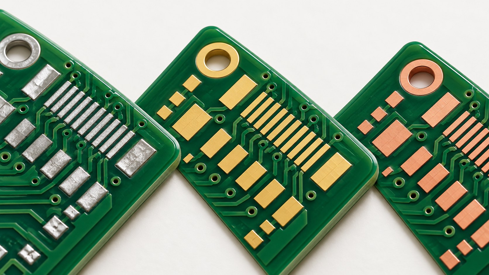
Table of Conent
Table of Conent
Choose HASL, ENIG, or OSP by the board’s least flexible requirement, then qualify that choice against the assembly schedule. A solder-coated HASL pad may suit a conventional assembly when its deposited profile is acceptable to the land pattern. ENIG offers a flatter metal surface and a nickel barrier where fine-pitch geometry or a specified contact function calls for them, but the plating and acceptance requirements must be controlled. OSP leaves a protective organic film over copper for soldering; its suitability depends particularly on the chosen chemistry, packaging, elapsed time, heat exposures, and any rework plan. None is the cheapest or most reliable finish in every assembled product. Before releasing a drawing, put the land geometry, contact areas, solder alloy, expected thermal sequence, board storage conditions, finish specification, and lot evidence in the same decision. Then compare the delivered PCBA cost rather than the bare-board finish surcharge alone.
Start with the pad, contact, and assembly requirements
The first disqualifier is the actual land or contact requirement, not a generic ranking of finishes. Identify the smallest component lands, any ball-grid-array or other fine-pitch sites, edge contacts, test pads, and surfaces that will be soldered in separate operations. Review the component vendor’s pad and assembly guidance along with the released PCB drawing. A flat-looking coupon in a supplier brochure does not establish coplanarity on the intended production land pattern.
If the design has a mating contact, state its electrical and wear requirements separately from solderability. ENIG is often considered when a planar soldering surface and nickel barrier are useful, but immersion gold on a solderable pad is not automatically a qualified wear surface. A connector designer may specify a different contact finish or plating process. If all exposed pads are soldered, ask whether the selected solder alloy, stencil, placement, and inspection process tolerate the profile and handling requirements of the candidate finish.
| Decision input | HASL | ENIG | OSP | Release evidence |
|---|---|---|---|---|
| Small, closely spaced lands | Qualify the solder deposit profile on the actual pattern; local excess or variation may matter. | Planar deposited metal is a common candidate; qualify the chosen plating and assembly process. | Thin organic coating preserves the underlying copper geometry; control handling and soldering sequence. | Land drawing, assembly trial or process evidence, inspection criteria. |
| Exposed electrical contact | Do not assume a solder-coated pad meets mating-contact requirements. | Check the specified nickel/gold stack and contact duty; solderable ENIG is not a universal hard-contact finish. | Do not assume an organic solderability coating provides a durable mating surface. | Connector/contact specification and supplier-approved finish for that area. |
| Long hold or multiple heat steps | Control oxidation, handling, and solderability for the agreed process. | Control plating quality, storage, and solderability; a metal finish does not remove all process risk. | Verify the exact OSP chemistry, pack, hold time, heat sequence, and rework route. | Process-specific shelf/thermal qualification and receiving or solderability records. |
| Lowest delivered assembly cost | Compare finish price with stencil, rework, inspection, and yield assumptions. | Compare plating premium with any process benefit it actually delivers. | Compare board price with handling, time, heat, and potential rework constraints. | Same drawing, quantity, route, and acceptance assumptions in each quote. |
This matrix is a screening tool, not a substitute for a supplier process qualification. An IPC-hosted lead-free HASL technical paper illustrates why deposit coverage and profile can be relevant, while the IPC finish specifications define different material systems. The correct choice can change with the solder process and land design.
Know what HASL, ENIG, and OSP put on the copper
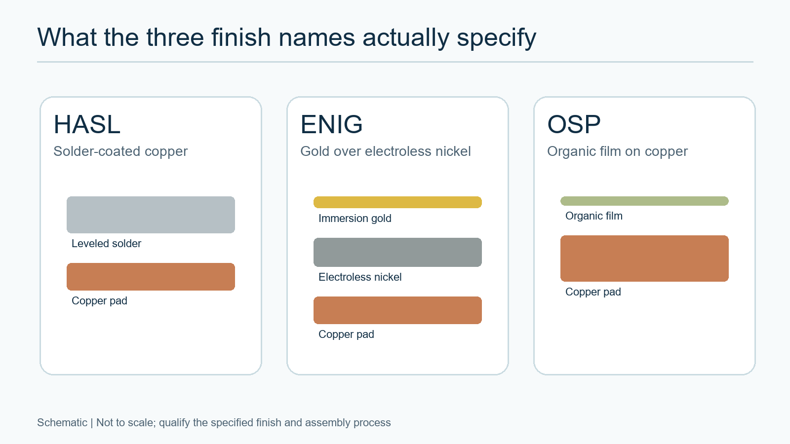
The three names describe different surfaces at the instant the board enters assembly. HASL applies solder to exposed copper and removes excess with heated air. Specify whether the project requires a lead-free or tin-lead process; “HASL” alone does not identify the alloy. The resulting solder layer must be assessed against the component lands and assembly method. The choice of alloy also needs to align with the product’s materials and compliance requirements; our lead-free and leaded solder assembly review explains why the whole assembly, rather than one label on the PCB quote, matters.
ENIG deposits electroless nickel and immersion gold on exposed copper. The gold protects the surface before soldering, while the nickel layer has a separate barrier and solder-joint role. IPC-4552B (April 2021) addresses ENIG requirements, including deposit and nickel-corrosion acceptance topics. Merely seeing a gold color does not verify those requirements. Obtain the agreed specification revision, process controls, and lot-level acceptance evidence rather than inventing a thickness or accepting a photograph as proof.
OSP uses an organic coating to preserve exposed copper for subsequent soldering. IPC-4555 (April 2022) concerns high-temperature OSP; it should not be read as proof that every OSP chemistry survives the same thermal route. A finish supplier’s process portfolio also shows that OSP formulations vary. Ask the fabricator which chemistry and qualified assembly window will be supplied. For another organic-finish comparison with a different purchasing question, see our OSP versus immersion-tin review.
Match the finish to storage, reflow, and rework
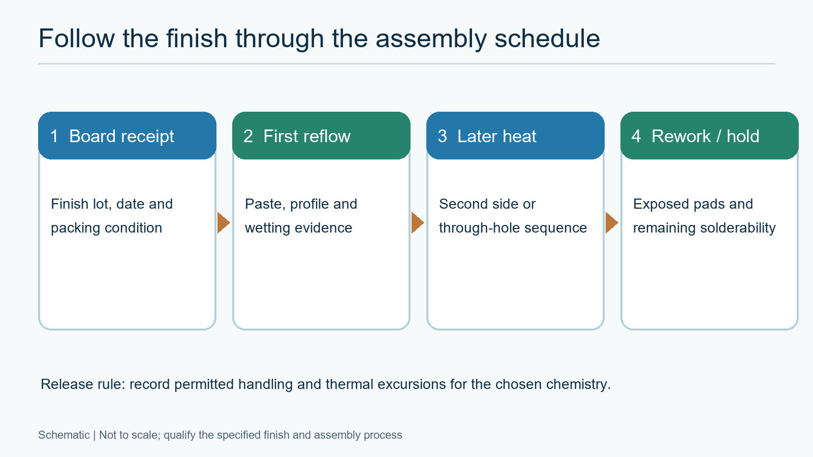
A finish decision remains conditional until the board’s time-and-temperature route is known. Document the date of fabrication, moisture-protective or other agreed packaging, shipping and receiving controls, time to first solder operation, subsequent wave or selective solder, reflow cycles, repair, and possible production hold. The number of thermal excursions is a process input, not a generic pass/fail count that can be inferred from a finish label.
When the pad map and intended heat sequence are available, share the pad map and assembly sequence for finish review. Include the fabrication drawing, solder alloy, expected hold interval, and any secondary solder or repair operation so the finish choice can be checked against the complete process before a board-only price is fixed.
For OSP, in particular, a later solder operation may encounter copper that has already seen heat or handling. Ask the assembler and fabricator to agree on the actual chemistry, allowable sequence, and action after a hold or opened package. For ENIG, planarity can help a land geometry without excusing plating defects or poor storage. For HASL, a stable solder deposit on one board type does not prove suitability for every pitch or stencil design. IPC J-STD-003D (January 2023) provides a printed-board solderability test framework; select the test method, sampling, and acceptance agreement appropriate to the purchase rather than writing “solderable” without a measurable basis.
The most useful receiving question is: “What evidence shows this lot is inside the finish and assembly window we actually specified?” Record a hold/release route for damaged packaging, unclear date code, unexpected heat exposure, or a solderability concern. A record from a different chemistry or a generic marketing shelf-life claim is insufficient for that decision. Our PCB solderability testing guide details the distinction between a finish selection and a tested lot.
Compare total assembled cost, not only the board quote
The economical finish is the one that meets the released design and process at the lowest credible delivered PCBA cost. A bare-board quote may make OSP or HASL look attractive, while a flat ENIG surface may justify its premium on a particular fine-pitch design. Neither comparison is complete until both suppliers quote the same land geometry, alloy, quantity, packaging, assembly route, and acceptance standard.
Build a side-by-side cost model with the finish line item, board yield and panel assumptions, packaging and inventory exposure, stencil or print adjustments, inspection effort, planned solder operations, rework policy, and expected risk of a hold. Use supplier-specific figures rather than published “typical” percentages. If one candidate requires an extra qualification trial, include it; if another requires a special contact-area process, quote that separately. The purchasing comparison should make the assumptions visible enough that engineering can reject an apparently low price when it omits a required operation.
The same principle applies to lot size. A prototype schedule with rapid assembly may have a different optimum from a long, staged build. A quoted shelf-life number cannot stand in for a packaging plan, and a lower finish surcharge cannot compensate for an unsupported contact requirement. Our PCBA quote breakdown shows why fabrication, sourcing, assembly, and testing assumptions need to be visible in the same request.
Put finish chemistry and acceptance evidence on the drawing
A purchase order should name the chosen process and what would make the delivered lot acceptable. The drawing or controlled fabrication notes should identify the surface finish, applicable revision of any called-up specification, exposed areas with different functions, and any required masking or selective finish. The assembly package should identify the solder alloy, thermal route, storage and pack requirements, receiving inspection or solderability method, and the disposition owner if a lot falls outside the agreed window.
| Release item | Supplier or OEM evidence | Decision enabled |
|---|---|---|
| Finished land/contact definition | Controlled drawing, land map, connector requirement, and explicit selective areas. | Reject a finish that cannot meet the solder or contact function. |
| Finish process and standard | Named HASL alloy, ENIG specification/revision, or OSP chemistry and qualification basis as applicable. | Compare like-for-like quotes and avoid a generic, ambiguous “gold” or “OSP” callout. |
| Storage and thermal route | Packaging, fabrication/pack dates, planned receiving-to-solder interval, solder steps, and hold/rework disposition. | Decide whether a lot can proceed, needs testing, or requires engineering review. |
| Acceptance and traceability | Agreed sampling/test method, finish or solderability records, lot ID, and nonconformance route. | Release boards on auditable evidence rather than appearance or an unqualified shelf-life claim. |
Use the named standards for their actual scopes: IPC-4552B for ENIG, IPC-4555 for the relevant high-temperature OSP process, and J-STD-003D for printed-board solderability test methods. The parties still need to specify contractual revisions, methods, samples, limits, and lot disposition. Do not import an unsighted numeric requirement from another revision into the drawing. If a supplier proposes an alternate finish, require an engineering change review of land geometry, contact behavior, process route, and acceptance evidence before treating the alternate as equivalent.
Release the board and assembly as one controlled decision
Selecting HASL, ENIG, or OSP is complete only when fabrication and assembly agree on the same controlled inputs. Start with the disqualifying land or contact need, then confirm the exact finish process, thermal and storage route, and acceptance record. Compare total assembled cost only among candidates that pass those requirements. This prevents a price-only substitution from creating a board that is difficult to print, solder, inspect, hold, or rework.
A full-turnkey build can align board fabrication, component sourcing, SMT and through-hole assembly, and specified test steps around one released package. Our full-turnkey PCB assembly overview describes that project scope. If a design is ready to quote, send the controlled fabrication and assembly package for review with Gerbers or fabrication files, the assembly drawing, BOM, quantities, required finish, planned solder and test route, and any hold or contact requirements. The engineering and quotation review can then surface finish assumptions alongside parts, assembly, and inspection scope before a production commitment.
Latest Blog

Contact Info
Phone: +86-755-82882936
Email: [email protected]
WhatsApp: +86-13570802455
Wechat: +86-13570802455
Address: 2nd floor,D Bldg.,Electric Link Technology Bldg.,Gongming,Guangming New Dist.,518106 Shenzhen, China