
IPC-2221C PCB Design Rules: Apply the Right Standard Before Release

Table of Conent
Table of Conent
IPC-2221C is the generic printed-board design standard, but it is not a complete, universal PCB rule deck. A release-ready design pairs the applicable revision of IPC-2221 with the board-technology sectional standard, the product’s electrical and environmental requirements, and the fabricator’s verified process limits. Before changing a CAD clearance or trace rule, record which requirement controls it, the geometry and operating conditions it assumes, and who will resolve a conflict. That approach is more useful than copying a clearance number from an unsourced online table.
The following framework is for designers and buyers preparing a real fabrication and assembly handoff. It does not reproduce proprietary IPC tables or certify that a particular board complies with a standard. The project team must consult the licensed, applicable documents and confirm the finished stackup and acceptance criteria with its chosen suppliers.
Start with IPC-2221C, then select the standards that fit the board
IPC-2221C supplies a generic design framework; a rigid, flexible, HDI or RF board can require additional, more specific design guidance. IPC’s design-standards catalog identifies IPC-2221 as generic and lists IPC-2222 for rigid organic boards, IPC-2223 for flexible boards, IPC-2226 for HDI and IPC-2228 for RF/microwave boards. Select by the actual construction, not by the standard number that happens to appear in an old drawing note.
The publicly available IPC-2221C table of contents identifies it as the Generic Standard on Printed Board Design and says it supersedes IPC-2221B. IPC’s release list places IPC-2221C in late 2023. A live project should still verify the revision of every other referenced document separately: IPC lists IPC-2223F as a 2026 release, illustrating why an inherited bill of standards can become inconsistent even when the generic document is current.
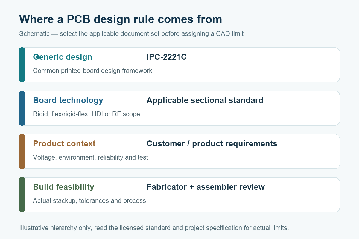
A product specification may impose electrical isolation, thermal, environmental or reliability requirements that are stricter than a generic design guideline. Conversely, a supplier may need a wider conductor, larger finished hole or different stackup than the CAD library’s nominal minimum to build a particular yield target. These are separate questions. The design authority should document the controlling requirement, while the fabricator confirms process capability and proposes any departure for approval.
Do not turn a clearance table into a universal spacing rule
Electrical spacing is a conditional design decision, not a single number that applies to every PCB. A clearance value has meaning only with the relevant voltage and waveform, conductor relationship, layer or surface, insulation system, environment and applicable product requirements. Distinguish an air gap from a path along an insulating surface; also distinguish an electrical-safety limit from a fabricator’s minimum imageable copper spacing. The smallest printable gap is not automatically the safe operating gap.
For a board with elevated potentials, identify the exact nets and their maximum working and transient conditions before assigning rules in CAD. Determine which product or safety standard governs the end application and what test or review evidence it requires. A separate high-voltage PCB spacing guide discusses creepage, clearance and slots in greater detail; this article focuses on how to keep the standard choice and decision ownership traceable at release.
A practical review separates three questions: What distance is required by the electrical design and applicable standards? What finished geometry will be present after copper etch, solder mask, routing and assembly? What evidence will show the released layout and supplied board meet the approved requirement? A solder-mask opening or a slot can change the physical path, but neither should be credited as an insulation feature without a project-specific engineering assessment. Keep the electrical limit and the manufacturing tolerance as separate entries in the rule record.
Turn a standard into a controlled rule record
A CAD rule is auditable when its source, assumptions, implementation and release evidence travel together. The table below is a project worksheet, not a table of IPC minimum values. Fill each row from the licensed standard, the released product specification and the supplier’s written capability review.
| Rule decision | Controlling input to confirm | CAD or drawing implementation | Release evidence and owner |
|---|---|---|---|
| Conductor-to-conductor spacing | Electrical conditions, applicable product standard and relevant IPC design guidance | Net-class clearance plus explicit exceptions for geometry and surface | Electrical owner approves the limit; fabricator checks finished spacing capability |
| Trace width and copper | Current, temperature-rise objective, layer location and chosen copper construction | Width rules tied to a named stackup revision and copper callout | Design owner provides assumptions; fabricator confirms copper and etch capability |
| Hole, pad and annular ring | Finished-hole need, plating, board type and assembly component data | Padstack and drill table with finished dimensions and tolerances | Fabrication drawing, drill output and unresolved-deviation log |
| Board edge and panel features | Enclosure constraints, depaneling process, connectors and assembly handling | Outline, keepouts, tooling and fiducial requirements in controlled files | Mechanical owner and supplier review the route and panel proposal |
| Controlled impedance | Signal target, reference plane, material and the fabricator’s achievable stackup | Named nets and an impedance table linked to a stackup drawing | Fabricator returns a proposed stackup and measurement plan for approval |
This worksheet prevents a common handoff failure: an engineer enters a CAD minimum from a general reference, while the drawing requests a different finished dimension and procurement quotes yet another stackup. A supplier cannot reconcile those requirements by simply accepting a file. The open issue should be dispositioned by the design authority and reflected in the next controlled release. In a PADS design-rule workflow, constraints are established before routing; that software discipline only works if the underlying requirements are themselves controlled.
If a released stackup or spacing assumption is uncertain, share the stackup and rule questions for manufacturing review with the proposed copper, layer count and critical net classes. Those inputs let the fabrication assumptions be checked before the remaining assembly scope is quoted.
Separate electrical need from fabrication capability
A fabricator’s capability statement answers what its process can repeatedly make; IPC-2221C helps frame design requirements, and the two should be reconciled rather than treated as interchangeable. Siemens’ PCB DFM discussion also emphasizes that a designer must account for the particular manufacturer’s process when turning specifications into DFM rules.
Consider an example: a designer’s working file uses a fine conductor/space setting that the selected fabricator can image only with a special process. The product may allow a wider space, but widening it affects a connector escape or controlled-impedance geometry. The correct response is a documented alternative stackup, route or process review. Quietly relaxing the DRC in one region, or quoting a different build without updating the released files, breaks the chain of evidence.
Ask the supplier to review the actual layers, copper weights, drill and finish requirements, route profile, impedance targets and panel constraints. For a simple rigid construction, the two-layer PCB design discussion can help frame stackup and routing tradeoffs. For HDI, flex or RF designs, use the applicable sectional guidance and qualified process review rather than assuming that the same rigid-board defaults apply.
Manufacturability is not only a bare-board question. Parts, land patterns, fiducials and test access can change an assembly plan even when the bare PCB can be fabricated. The relevant full-turnkey PCB assembly scope illustrates why fabrication, component sourcing and assembly requirements should be aligned in a single quotation package instead of resolved by disconnected vendors after design release.
Release one build package for fabrication and assembly
A usable release contains the controlled design data plus the decisions that cannot be inferred from copper images. The fabricator needs an unambiguous board revision, stackup, materials, finished dimensions and tolerances, hole and plating data, surface finish, mask, outline, special features and inspection expectations. If impedance or electrical spacing is critical, identify the relevant nets or areas, target conditions and approved test or review method instead of leaving the supplier to reverse-engineer the intent.
Gerber files may be sufficient for copper and artwork only when companion drawings and drill data close the remaining questions. An intelligent data package can carry richer layer and feature relationships, but it still needs revision control and a clear specification. The Gerber, ODB++ and IPC-2581 comparison explains those transfer choices. Whichever format is used, send one approved revision and log every accepted supplier query against it.

When assembly is in scope, pair the board release with a revision-matched BOM, component alternates policy, pick-and-place or centroid file, assembly drawing, programming and test requirements, quantities, and packaging or traceability needs. A footprint or panel change made to satisfy a bare-board process can affect placement, soldering or test access. The assembler should therefore see the fabricator-approved construction before confirming its own process plan.
For procurement, ask what evidence is actually being purchased. A drawing note that says “build to IPC-2221C” names a design reference, but it does not by itself specify a finished-board acceptance class, a product safety evaluation or a measured result for this lot. State the applicable fabrication and assembly acceptance documents, customer deviations, evidence to be supplied and who can approve a change. Do not imply that a design-standard reference is a certificate.
Once the rule sources, supplier exceptions and project files are resolved, send the released board and assembly package, including Gerber or equivalent data, the stackup and critical rules, BOM, placement files, quantity and test scope. That gives OrinewPCB enough context to evaluate the fabrication, sourcing, assembly and test assumptions together for a project-specific quote.
What to verify before signing off the design rules
Sign-off should confirm a decision chain, not simply a green DRC report. Check that the generic and sectional standards named in the release are the intended revisions, that product-specific electrical and environmental limits have owners, and that the supplier has accepted or formally queried the actual stackup and feature set. Review any waived CAD checks, drawing notes and controlled outputs for contradictions. Keep the approved disposition with the released revision.
IPC-2221C is a useful starting point because it provides common printed-board design language. The dependable outcome comes from applying it alongside the right sectional and product requirements, confirming achievable manufacturing geometry, and transferring one controlled set of decisions to fabrication and assembly. A team that cannot identify the source and owner of a critical rule should resolve that gap before calling the design ready for production.
Latest Blog






Contact Info
Phone: +86-755-82882936
Email: [email protected]
WhatsApp: +86-13570802455
Wechat: +86-13570802455
Address: 2nd floor,D Bldg.,Electric Link Technology Bldg.,Gongming,Guangming New Dist.,518106 Shenzhen, China