
MWD PCB Depaneling: Qualify Support and Strain
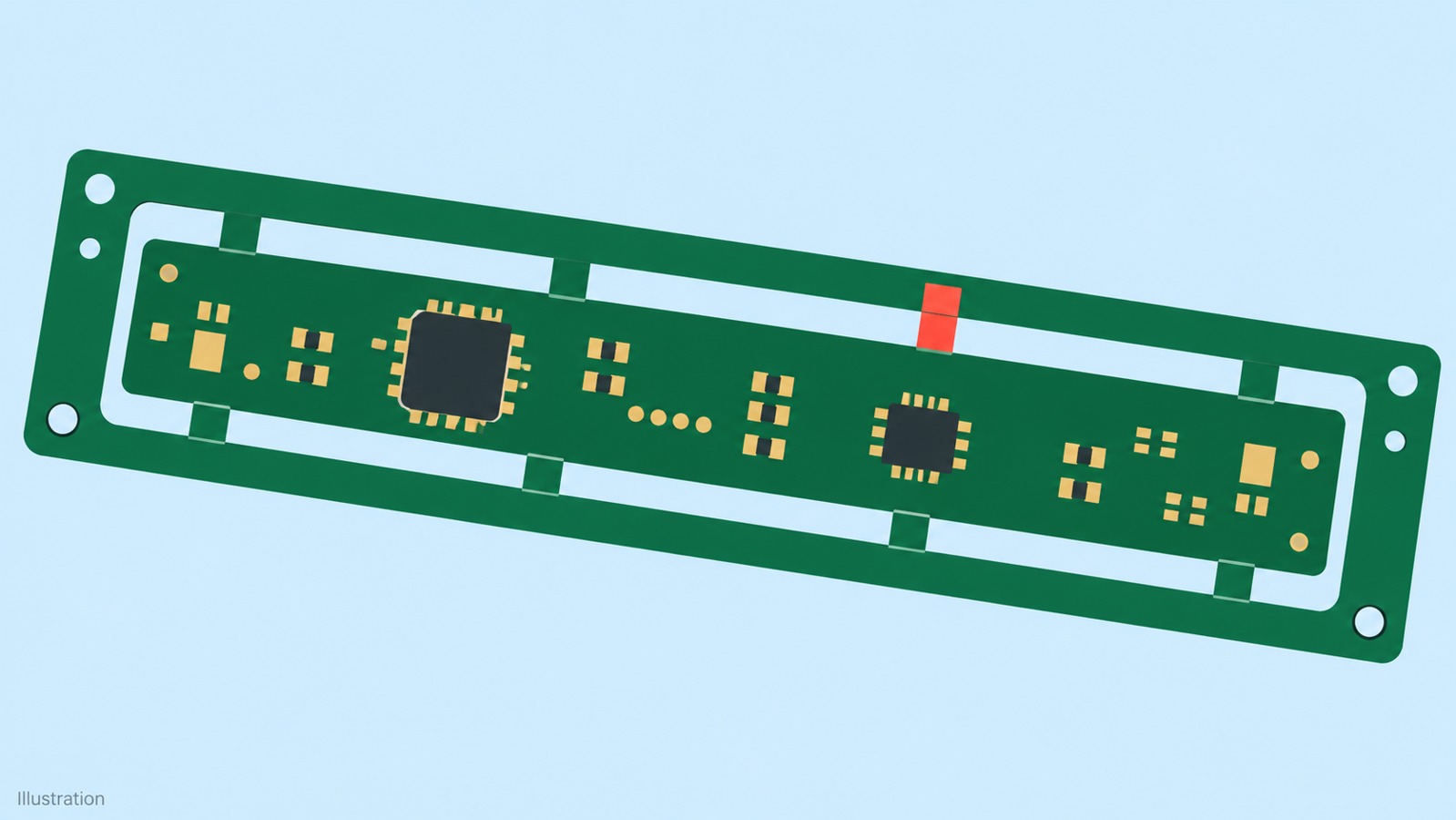
Table of Conent
Table of Conent
MWD PCB depaneling should be qualified as a controlled manufacturing process: define the panel connections, cutting method, supports, removal sequence, and component-specific strain criteria before releasing production. Measurement-while-drilling electronics may face demanding service conditions, but a downhole rating does not establish how much board bending is acceptable during separation. A visually straight board or an immediate electrical pass also cannot replace evidence that the chosen process protects vulnerable components and interconnects.
The practical release connects a panel revision to a fixture and process revision, measured strain records, applicable component guidance, and post-cut acceptance checks. Test the changing support conditions as neighboring boards and remaining tabs are removed; do not characterize only the first cut. Keep this manufacturing evidence separate from chassis integration, environmental qualification, and any assessed safety configuration. The framework below applies to the actual board geometry and BOM, without prescribing a universal strain limit.
Treat depaneling as a manufacturing load case
Evaluate the separation process independently from the product’s service qualification. Its loads occur while the board is held, cut, released and transferred, often under different constraints from those inside the completed tool.
Honeywell’s downhole electronics packaging overview describes MWD control and data acquisition, including compact packaging for harsh environments. That context makes manufacturing damage consequential; it does not provide depaneling limits for another manufacturer’s assembly.
When a design uses a long, narrow board, examine unsupported spans and the direction in which the board can rotate as connections disappear. Other MWD geometries need their own review. Mark ceramic capacitors, area-array packages, connectors, sensors and mechanically constrained features on the assembly drawing. Include both sides: an accessible top surface does not guarantee clearance for an underside component or fixture support.
Separate collision risk from flexure risk. A tool or hold-down striking a part needs a clearance correction; a clear tool path can still bend the board. Record these as different review items so a successful interference check is not mistaken for complete process qualification.
Choose the panel and separation method together
Select the separation method with the panel layout and fixture access, rather than maximizing boards per panel first. The relevant comparison is the complete supported process and its acceptance evidence, not the method name alone.
The PCB panelization overview introduces panel terminology and common layout features. Carry the selected supplier’s approved dimensions and the assembly’s actual constraints into the process review.
Eurocircuits’ customer-panel guidance distinguishes break routing and V-cut scoring and explains the role of retained tabs and panel borders. Its dimensions are supplier-specific. For the selected fabricator, obtain an approved panel drawing that identifies the separation features and the finished board profile.
| Route under consideration | Process definition needed | Decision evidence |
|---|---|---|
| V-scored panel | Score geometry, supported separation operation, blade and hold-down clearance | Does the actual operation meet component guidance without interference? |
| Routed outline with retained tabs | Tab locations, final cutting method, support contacts and removal order | Are intermediate states and final pickup controlled, as well as the initial cut? |
| Individual board in an assembly carrier | Carrier contacts, loading, thermal-process compatibility and unloading | Does avoiding panel separation introduce different handling or assembly constraints? |
Murata’s MLCC layout guidance for board bending shows why component orientation and separation-region geometry matter. Its illustrated slit and orientation examples address particular deformation conditions. Treat them as design-review inputs, not a guarantee that rotating a capacitor or adding a slit makes every cutting process acceptable.
The official OrinewPCB clip below explains how board bending can contribute to ceramic-body microcracks. YouTube identifies it as AI-generated; it is an explanatory illustration, not a depaneling demonstration, inspection record, or MWD qualification result.
Qualify every support state before freezing the process
Review how the load path changes through the approved cutting sequence. The first, intermediate and final retained connections can produce different boundary conditions; measurement and engineering review should identify the critical state instead of assuming the last tab is always worst.
Create a support-state sheet using the actual panel drawing. For each selected state, mark remaining connections, fixture contacts, clamps, tool clearance, component locations and the intended pickup point. Check what changes after an adjacent board is removed. A support that was reachable beneath the full panel may no longer restrain a released individual board.
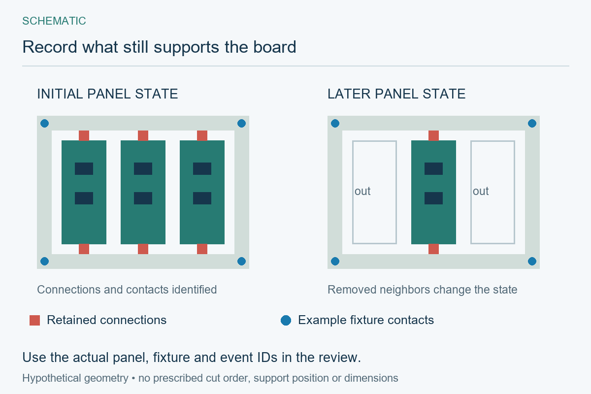
Include loading, clamping, cutting, unclamping and transfer in the review. Where strain monitoring is required, identify each operation in the saved record so an event can be connected to its support state. Use the PCB assembly drawing checklist to keep mechanical constraints and handling notes with the controlled build information.
Once the proposed panel and handling route are defined, share the panel drawing and support-access constraints with the component map so fabrication and assembly assumptions can be reviewed before tooling and production scope are fixed.
Match the strain metric to the component guidance
A strain reading and an acceptance limit must describe the same metric and conditions before they can be compared. The unit “microstrain” alone does not establish compatibility. Record the component, source revision, sensor location, coordinate reference, metric and any rate-dependent conditions.
The public IPC/JEDEC-9704A scope and contents, dated February 2012, describe strain-gage methodology for assembly, test and handling operations. They distinguish strain metrics and reporting topics. This public sample supplies methodological context, not a universal numerical acceptance criterion for the current project.
Two original vendor documents illustrate the compatibility problem. NI’s PCB strain-measurement guide, updated May 2026, presents a common principal-strain versus strain-rate reporting chart. Intel’s March 2016 board-flexure methodology specifies maximum calculated diagonal strain for comparison with its applicable BFI guidance and says not to substitute principal strain. It also limits those guidance values to transient manufacturing bend conditions.
These are different guidance contexts, not interchangeable numbers. The Intel example does not establish that an MWD BOM contains Intel devices or that its criteria apply downhole. Obtain the actual component supplier’s applicable guidance and have the responsible engineer approve the measurement method and comparison. If the required metric or criterion is missing, report the measurement as characterization rather than a passing qualification.
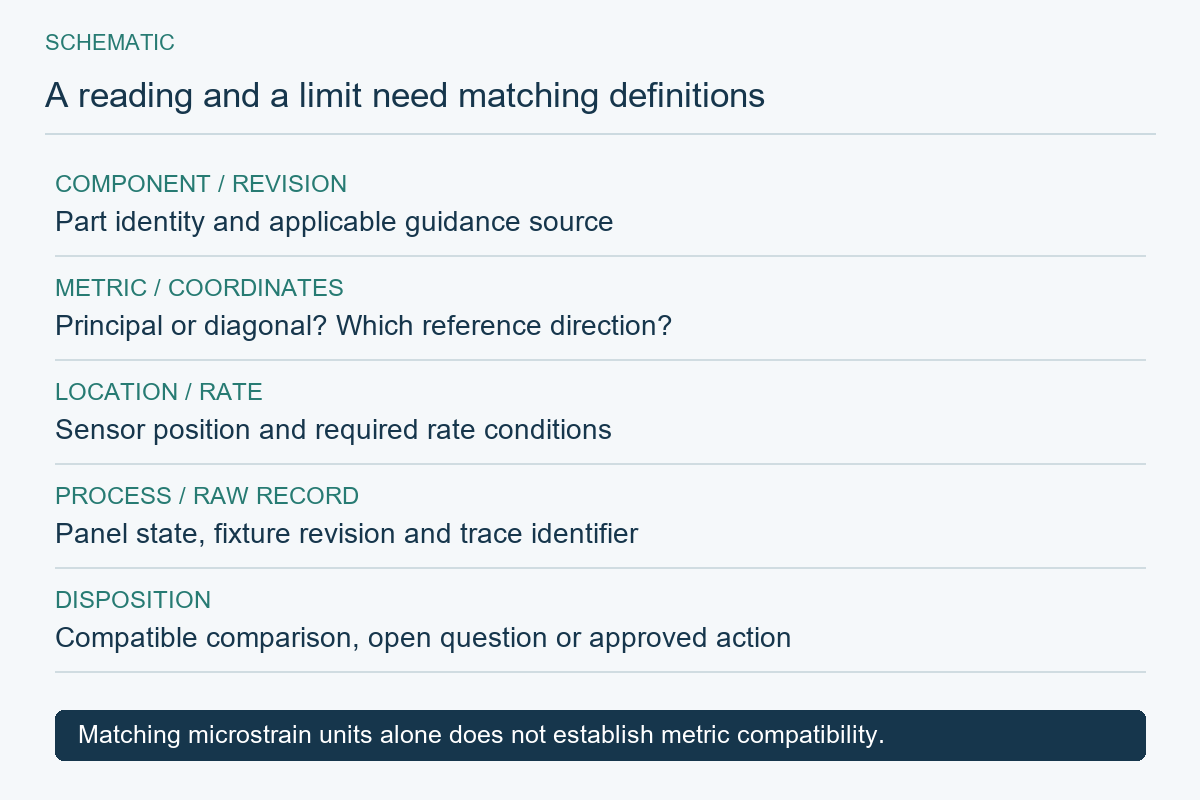
Keep the raw time record with the processed result and the support-state identifier. Document instrumentation setup, checks and processing choices needed to reproduce the analysis. If two suppliers report different metrics, ask for compatible analysis from the original records; do not compare the displayed peaks as if they were equivalent.
For example, a fixture revision may reduce the reported principal-strain peak while the agreed component guidance requires a different metric. That result can support process investigation, but it cannot close the acceptance requirement until the correct comparison is available. Preserve both the original result and the reviewed disposition.
Separate post-cut release from downhole qualification
Release the manufacturing process against its approved baseline, then retain the separate product-level evidence required for service. Neither a lower strain peak nor successful depaneling proves that the completed assembly meets its temperature, shock, vibration or safety requirements.
| Question | Evidence to agree | Responsible decision |
|---|---|---|
| Is separation controlled? | Panel and fixture revisions, support-state records, applicable strain comparison | Process/quality approval of the manufacturing baseline |
| Is this delivered board acceptable? | Required post-cut inspection and electrical records, lot and revision identity | Lot release against the purchase specification |
| Does the installed assembly meet service needs? | Approved chassis, mounting and environmental verification | Product qualification authority |
| Does a change affect an assessed safety configuration? | Controlled design record and authorized change assessment | Responsible design or assessment authority |
This is a proposed responsibility matrix, not a claim that every MWD assembly uses the same certification route. Depaneling does not establish intrinsic safety. Any applicable assessed construction, restricted material choice or safety-critical spacing must remain under its authorized design controls.
Agree the post-cut checks before the pilot build. They may include finished-profile and edge inspection, relevant component and termination observations, and electrical tests specified for the assembly. An electrical pass answers the tested electrical question; it does not by itself rule out every mechanical defect. Investigate suspect damage using a qualified analysis plan rather than diagnosing internal cracks from an illustration.
Record changes to the panel outline, tab pattern, support contacts, cutting program, laminate construction, component package or handling route. Review their effect on the approved evidence and decide whether additional characterization or qualification is needed. Keep the approval and affected revisions identifiable instead of treating a repeat order as automatically equivalent.
Choose pilot specimens to represent the process variations that the review identifies. Array position, removed neighbors, tool condition and operator transfer can be relevant variables. Do not take every recorded result from one convenient location and assume that it represents the whole panel. Agree the selection rationale and required evidence with quality engineering; this framework does not prescribe a universal sample count.
Release the panel and assembly package together
A usable depaneling release connects the actual board, panel, fixture, separation route and acceptance evidence. The full turnkey PCB assembly service is a starting point for coordinating fabrication, sourcing, assembly and test requirements; special tooling and qualification work need project-specific confirmation.
For a complete build review, provide the controlled panel files and assembly acceptance requirements with the BOM, placement data, mechanical mounting information, quantities and target schedule. Include the approved process constraints and any open evidence questions. That gives the quotation a defined scope while keeping manufacturing release and downhole qualification tied to their respective requirements.
Latest Blog
Contact Info
Phone: +86-755-82882936
Email: [email protected]
WhatsApp: +86-13570802455
Wechat: +86-13570802455
Address: 2nd floor,D Bldg.,Electric Link Technology Bldg.,Gongming,Guangming New Dist.,518106 Shenzhen, China