
PADS PCB Workflow: Set Layers, Design Rules and Libraries Before Routing
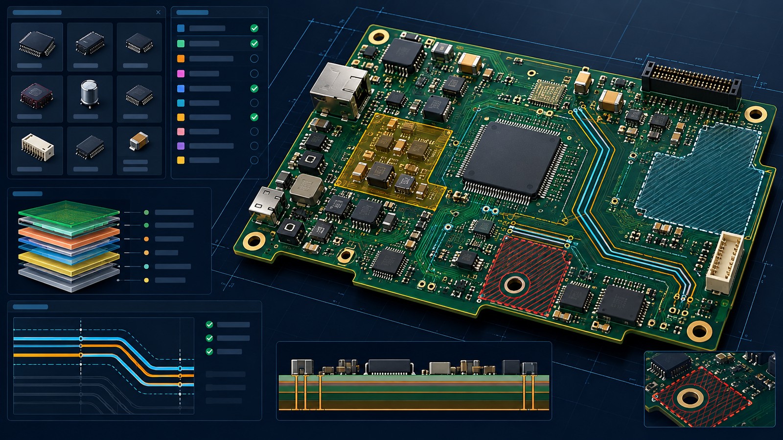
Table of Conent
Table of Conent
A productive PADS PCB workflow starts before the first trace is routed. Define the board structure, manufacturing limits, component data, placement constraints, and electrical rules first. Then route inside a controlled design space and verify the outputs against the same requirements. This order prevents late discoveries that force layer changes, footprint replacement, rerouting, or a new fabrication release.
This guide focuses on the decisions that connect PADS layout work to a manufacturable PCB assembly: layer planning, libraries, constraint classes, placement, routing, verification, and release data. The exact commands vary by PADS product and version, but the engineering sequence remains stable.
1. Freeze the design inputs and ownership
Begin with an approved schematic, preliminary BOM, mechanical outline, connector locations, mounting holes, keepouts, height limits, and product requirements. Identify which nets are power, clocks, differential pairs, high current, sensitive analog, RF, or safety related. Record the target board technology, expected copper weight, minimum feature assumptions, impedance needs, and test strategy.
Assign owners for electrical constraints, mechanical data, component approvals, and manufacturing release. A layout designer should not have to infer an impedance target from a marketing document or select an alternate package during routing. Open decisions belong in a tracked issue list with a due date and responsible engineer.
The applicable standards and contract requirements should be named, not assumed. IPC lists IPC-2221 and related sectional standards within its PCB design standards. The revision table currently identifies IPC-2221C as the 2023 revision, so teams should verify the revision cited by their customer or quality system rather than relying on an old template.
2. Define the board outline, stackup, and layers
Import or create the mechanical outline from controlled data. Verify units, origin, cutouts, slots, edge clearances, connector projections, and mounting features. Lock critical geometry or place it on a controlled layer so a routine placement edit cannot move it accidentally.
Set the layer stack before detailed routing. The fabricator should confirm available laminates, dielectric thicknesses, copper weights, finished board thickness, via structures, and controlled-impedance construction. Do not treat a generic CAD stack as a manufacturing stackup. Plane assignments and signal-layer references affect return paths, impedance, crosstalk, and routability.
Create a layer-use table that states the purpose of each copper and documentation layer. Include signal direction guidance where it helps, power and ground assignments, solder mask, paste, silkscreen, assembly outlines, fabrication information, and mechanical notes. For rigid-flex or special constructions, identify bend regions and material transitions before placement.
3. Verify libraries before placement
Every placed component should resolve to an exact approved part and a verified footprint. Check pin numbers, pad numbers, package suffix, pad geometry, pin-one orientation, paste openings, courtyard, origin, rotation, assembly outline, and 3D model alignment. Use the controlled process described in PCB library quality verification.
Resolve missing or provisional footprints before they enter dense placement. A temporary footprint can distort escape routing, keepouts, thermal behavior, enclosure clearance, and BOM-to-placement consistency. When an alternate part is allowed, confirm that its package, pinout, height, and assembly requirements match the released design rules.
Keep the library revision traceable in the design or release manifest. A library update after routing requires an impact review. It may change pad position, body clearance, centroid origin, rotation, or pin mapping even when the visible component name stays the same.
4. Build design rules and constraint classes
Translate manufacturing and electrical requirements into constraints before routing. At minimum, define trace widths, clearances, via types, drill limits, annular-ring expectations, copper-to-edge spacing, solder-mask rules, and allowed routing layers. Add net classes for power, analog, clocks, differential pairs, controlled impedance, and other circuits that need distinct treatment.
Siemens describes PADS Professional as a constraint-driven environment in which mechanical rules such as widths, clearances, and allowed layers can be combined with electrical rules such as length or delay. Its routing automation overview explains that constraints are entered before interactive or sketch routing so the router can maintain them during editing.
Use a clear hierarchy. A broad default should cover ordinary nets, while specific classes and exceptions override it intentionally. Review class-to-class spacing matrices, rule areas, and component-specific constraints. Conflicting or overly broad overrides can make a nominally complete rule set ineffective.
Before detailed routing starts, share the preliminary stackup, board outline, BOM, and critical constraints with the manufacturing team. Early feedback can expose unavailable materials, unsupported via structures, stencil risks, or clearance assumptions while changes are still inexpensive.
5. Place components for signal flow and assembly
Place fixed mechanical components first: connectors, switches, displays, sensors, mounting hardware, heatsinks, and enclosure interfaces. Next place critical functional groups using the schematic and current-return paths as guides. Keep decoupling components close to the pins they serve, minimize high-current loop area, and separate noisy switching nodes from sensitive analog circuitry.
Placement must also support assembly and inspection. Confirm component-to-component spacing, tool and nozzle access, polarity visibility, rework access, fiducials, panelization features, and test-point reach. Avoid trapping small parts beside tall hardware or placing connectors where cables cannot be installed after enclosure assembly.
Use 3D review for mechanical clearance, but do not treat a clean 3D image as proof of manufacturing readiness. Check real package heights, mating envelopes, tolerance stackups, and installation sequence. Record unusual orientation or hardware requirements in the PCB assembly drawing.
6. Plan routing before routing
Review congestion, escape paths, reference planes, via strategy, and layer transitions. Fan out dense packages with the selected fabrication capability in mind. Route the most constrained circuits first: clocks, differential pairs, memory buses, RF, high-current paths, and sensitive analog nets. Ordinary control signals can follow after the critical topology is stable.
The Siemens physical-layout overview describes how PADS Professional carries mechanical and electrical constraints into placement and interactive routing. Use automation to enforce known rules, then review the result for current return, coupling, stubs, plane discontinuities, and manufacturability. A route can be DRC-clean and still be poor engineering.
For differential pairs, confirm pair membership, impedance geometry, gap, allowed layers, via transitions, and length or delay rules. For power, verify current capacity, neck-downs, thermal reliefs, copper pours, and connection integrity. For mixed-signal designs, protect converter references, sensor inputs, and return paths from switching currents.
7. Run verification as a continuous loop
Run DRC throughout layout, not only at the end. Investigate every violation and every waived exception. Use named waivers with engineering justification rather than deleting rules to obtain a clean report. Re-run checks after placement changes, plane edits, tuning, footprint updates, and mechanical imports.
Verification should include unrouted connections, clearances, width and via rules, differential-pair constraints, length or delay rules, plane connectivity, copper islands, solder-mask slivers, silkscreen overlap, board-edge spacing, component height, and 3D collision. Add pre-layout and post-layout signal-integrity analysis where the interface risk warrants it.
Coordinate electrical verification with the manufacturing release automation described in automated ERC, DRC, and file release. Archive the rule set, report, tool version, design revision, and output hashes together so a later reviewer can reproduce the release state.
8. Generate and compare manufacturing outputs
Generate fabrication data, drill files, netlist or intelligent manufacturing data, fabrication drawing, assembly drawings, BOM, centroid file, and test documentation from one approved revision. The article on Gerber, ODB++, and IPC-2581 explains the tradeoffs among common fabrication data packages.
Do not rely on successful export as verification. Open the outputs in an independent viewer, confirm layer polarity and alignment, inspect drills and slots, compare copper and mask openings, and reconcile designators, quantities, side, rotation, and manufacturer part numbers across the BOM and placement file. Confirm that documentation layers and notes match the board revision.
Include a release manifest that names every delivered file, its revision, generation time, and purpose. Remove obsolete alternatives from the delivery folder so manufacturing does not have to guess which drill file, BOM, or drawing is current. If a file must be regenerated, repeat the output comparison and replace the manifest as one controlled release rather than mixing old and new artifacts.
| Gate | Required evidence | Release risk if skipped |
|---|---|---|
| Inputs | Approved schematic, BOM, outline, constraints, and owners | Layout built on changing assumptions |
| Stackup | Fabricator-reviewed materials, copper, vias, and impedance plan | Reroute or fabrication hold |
| Libraries | Approved symbols, footprints, part numbers, and revision record | Wrong package or pin mapping |
| Placement | Electrical, mechanical, assembly, and test review | Clearance and access failures |
| Routing | Constraint classes, topology review, and resolved DRC | Signal, power, or manufacturing defects |
| Outputs | Independent viewing, file reconciliation, and release manifest | Incomplete or mismatched production data |
When the package passes these gates, provide the released fabrication and assembly files with quantities, approved substitutions, test requirements, target delivery, and any special process notes. The PCB assembly team can then evaluate DFM, sourcing, stencil and assembly controls, inspection, and test scope against a stable data set.
Use the workflow as a release system
PADS features can accelerate placement, constraint management, and routing, but the result depends on the order and quality of the inputs. Establish the stackup, library data, and rules first. Place for electrical function and assembly. Route the critical circuits inside controlled constraints. Verify continuously, then compare every manufacturing output with the approved design. That workflow reduces avoidable iteration and gives fabrication and assembly teams a release package they can act on.
Technical references: Siemens PADS Professional Premium overview, Siemens routing automation, Siemens physical layout, IPC design standards, and the IPC document revision table.
Latest Blog







Contact Info
Phone: +86-755-82882936
Email: [email protected]
WhatsApp: +86-13570802455
Wechat: +86-13570802455
Address: 2nd floor,D Bldg.,Electric Link Technology Bldg.,Gongming,Guangming New Dist.,518106 Shenzhen, China