
Continuous Inkjet Controller PCB: Link Fabrication Checks to Final Test
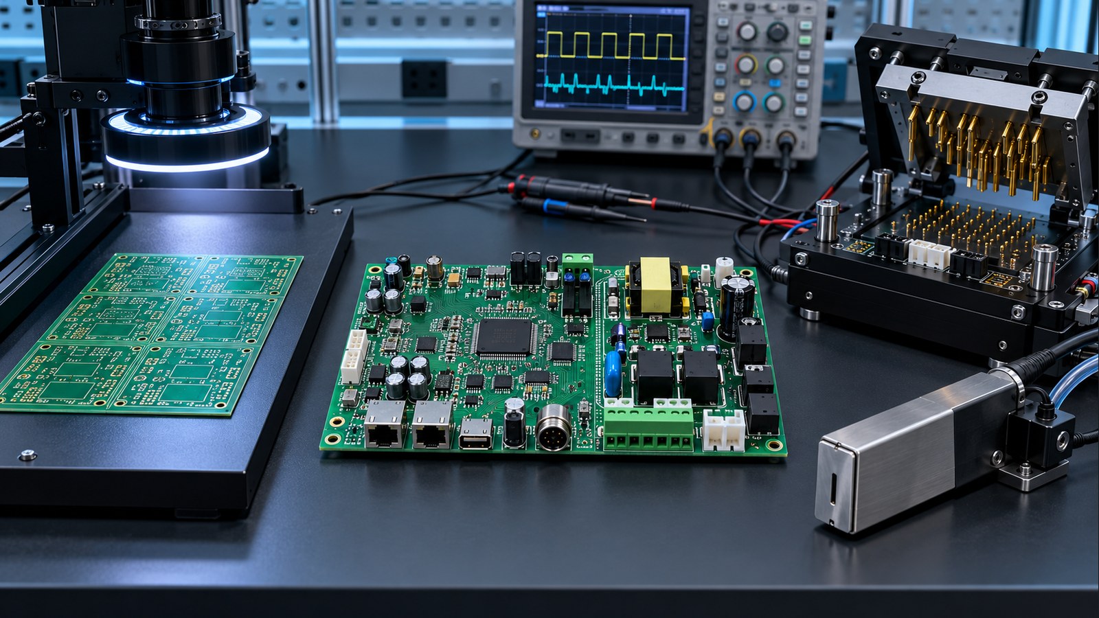
Table of Conent
Table of Conent
Continuous Inkjet Controller PCB: Link Fabrication Checks to Final Test
A continuous inkjet controller PCB should be tested as one traceable chain, not as separate bare-board, assembly, and final-test events. Fabrication checks must protect the structures that final function depends on: power integrity, isolation, plated holes, controlled interfaces, and test access. Assembly inspection must then confirm component identity, solder quality, polarity, and workmanship before powered tests exercise the pumps, valves, charging or deflection circuits, sensors, communications, and safety interlocks. The final test should trace every failure back to a controlled requirement, test point, and build record.
This linkage reduces the common gap in which a board passes continuity and visual inspection but fails only after it is connected to the printer harness. It also avoids asking functional test to detect hidden fabrication defects that should have been screened earlier.
Start with a requirements-to-test matrix
Define each critical function, its risk, the manufacturing stage that can create the defect, and the earliest practical verification. A CIJ controller may include low-voltage logic, motor or pump drivers, valve outputs, heater control, sensor inputs, communications, isolated interfaces, and a higher-voltage printhead section. Each block needs explicit limits rather than a generic “functional test passed” result.
For every requirement, record the evidence owner: fabrication certificate, electrical test record, incoming inspection, AOI, X-ray, in-circuit test, programming log, boundary scan, functional fixture, or system test. Include the design revision, BOM revision, firmware version, fixture revision, test-software version, and serial number. If a test is intentionally omitted, document why the remaining controls cover the risk.
The PCB assembly drawing checklist is a useful starting point for turning design intent into polarity, process, inspection, and test instructions that follow the build.
Fabrication checks should protect the final-test signal path
Bare-board acceptance begins with the construction and performance class specified by the product owner. IPC released IPC-6012F for qualification and performance of rigid printed boards, including requirements affecting plated structures, dielectric spacing, solderability, and microsection evaluation. The applicable class, board type, addendum, and deviations must be stated in procurement documentation.
Link those requirements to the CIJ circuit risks. Verify continuity and isolation for every net, including guard or high-voltage regions. Use coupons or production evidence for plating and dielectric structures when required. Check finished copper, hole size, annular ring, solder mask, surface finish, impedance where applicable, and board cleanliness. A certificate does not replace product-specific acceptance limits.
High-voltage or fast-switching sections need particular attention to conductor spacing, mask registration, contamination, sharp copper features, and connector separation. Do not apply a generic hipot voltage without confirming component ratings and the intended insulation system. Define which components or circuits must be disconnected, ramp rate, dwell, leakage limit, and discharge method.
Incoming and assembly inspection should prevent avoidable powered failures
Before assembly, verify the bare-board revision, stackup record, surface finish, electrical-test status, and any lot-specific coupon results. At kitting, control substitutions for drivers, optocouplers, isolation components, power supplies, sensors, connectors, and protection devices. Record moisture-sensitive handling and programming variants where they affect the process.
During assembly, use solder-paste inspection and AOI where they provide useful coverage. X-ray is valuable for hidden joints such as bottom-termination components and BGAs, but the inspection criteria must match the package and risk. The related AOI, X-ray, and ICT quality-plan guide explains how these methods complement rather than replace each other.
IPC-A-610J describes visual acceptability requirements for electronic assemblies, while J-STD-001 defines soldered-assembly requirements and evaluation methods. IPC notes that the two standards are developed in synergy through its J-STD-001 and IPC-A-610 validation program. State the contractual revision, class, and any customer-defined exceptions instead of writing only “IPC compliant.” Visual acceptance also does not replace electrical verification, hidden-joint criteria, cleanliness requirements, or the product-specific functional limits needed for a CIJ controller.
Design test access before the layout is frozen
Test coverage is a layout input. Provide accessible ground references and nodes for input rails, regulated supplies, reset, clocks, communications, key sensor inputs, driver outputs, and critical feedback. Avoid placing test pads where probes can short adjacent high-voltage or power nodes. Define pad finish, diameter, spacing, side, keep-out, and fixture approach with the test provider.
In-circuit test can find opens, shorts, wrong values, and some device-orientation faults. Boundary scan may improve digital coverage when supported by the devices and netlist. Neither proves that pumps, valves, charging circuits, sensing, or communications operate correctly under realistic load. Allocate each defect to the least expensive reliable screen.
If the board and fixture are ready for manufacturing review, provide Gerbers, netlist, BOM, placement data, schematics, test-point map, programming files, electrical limits, and representative loads through the controlled build-package submission. That enables fabrication, sourcing, assembly access, fixture needs, and test coverage to be reviewed together.
Build final test in safe, observable stages
A final functional test should progress from low-risk checks to energized loads. Begin with unpowered resistance and short checks. Apply current-limited power, confirm input current, and verify each regulated rail before releasing reset or enabling outputs. Program firmware and record verification or checksum data. Then exercise communications, sensors, and outputs with safe representative loads.
- Confirm fixture, harness, firmware, and board revisions.
- Run unpowered shorts and resistance checks.
- Power from a limited supply and verify startup current and rails.
- Check reset, clock, memory, and communications.
- Stimulate sensor inputs across defined thresholds.
- Drive pumps, valves, heaters, or simulated loads while measuring current and waveform behavior.
- Test interlocks, alarms, fault recovery, and safe shutdown.
- Record results by serial number and restore the required shipping state.
Use actual printhead hardware only when the test setup can control fluid, high voltage, discharge, cleaning, and waste safely. Otherwise, use validated simulators for production screening and reserve integrated printer tests for sampled or higher-level acceptance.
Set quantitative limits and guard bands
Every measurement needs units, limits, timing, and conditions. Specify input voltage, ambient range, warm-up time, load, firmware state, sampling method, and acceptable tolerance. A rail that is acceptable at no load may collapse when a valve or pump switches. A communication interface may pass a loopback but fail with the intended cable and grounding.
Base limits on the design, component data, and system requirements. Do not derive production limits from a single golden board. Use characterized samples to understand normal variation, then set limits that detect defects without rejecting healthy assemblies. Lock fixture calibration and reference-load maintenance into the control plan.
Solderability evidence can also connect fabrication and assembly risk. The PCB solderability testing guide explains how storage, surface condition, wetting tests, and process evidence should be interpreted before defects reach final test.
Make failure data actionable
Use failure codes that identify the stage, requirement, node, measured value, limit, fixture, and revision. “No power” or “functional fail” is too broad for corrective action. Preserve the first-failure result before rework, because repeated power cycles or probe contact can change the symptom.
When a failure occurs, separate product defects from fixture, software, cable, operator, and reference-load issues. Rework instructions should define permitted actions, inspection after rework, and the full or partial retest required. Trend recurring failure modes by lot and revision, but do not hide isolated safety or high-voltage defects inside yield percentages.
Release package and acceptance checklist
A production-ready CIJ controller package should include controlled Gerbers or ODB++, drill and netlist data, fabrication drawing, stackup, assembly drawing, BOM, placement data, firmware, programming instructions, test specification, limits, fixture interface, labeling, and traceability requirements. The PCB assembly service overview shows why fabrication, sourcing, SMT/THT assembly, inspection, programming, and test must use the same released data.
- Critical functions and manufacturing risks map to specific tests.
- Bare-board class, type, construction, and deviations are explicit.
- AOI, X-ray, ICT, programming, and functional coverage do not duplicate or leave gaps.
- Test points and fixture access are designed into the layout.
- Power-up is current-limited and high-voltage testing includes safe discharge.
- Limits, calibration, software, fixtures, firmware, and results are revision controlled.
- Rework and retest rules preserve traceability.
When the release set is complete, send the fabrication files, BOM, placement data, firmware, quantities, fixture concept, loads, and acceptance limits through the complete PCBA test-scope intake. Engineering and sourcing teams can then confirm testability, identify missing controls, and prepare a quote tied to the actual printer interfaces.
Conclusion
Reliable continuous inkjet controller PCB testing starts before assembly. Fabrication requirements protect the physical paths; inspection and in-circuit methods screen assembly defects; staged functional testing proves powered behavior under defined loads. When every result is tied to a requirement, revision, fixture, and serial number, failures become actionable and the final test stops being an expensive catch-all.
Latest Blog


Contact Info
Phone: +86-755-82882936
Email: [email protected]
WhatsApp: +86-13570802455
Wechat: +86-13570802455
Address: 2nd floor,D Bldg.,Electric Link Technology Bldg.,Gongming,Guangming New Dist.,518106 Shenzhen, China