
HDI PCB Release: Connect BGA Escape, Microvias, and Build-Up Layers
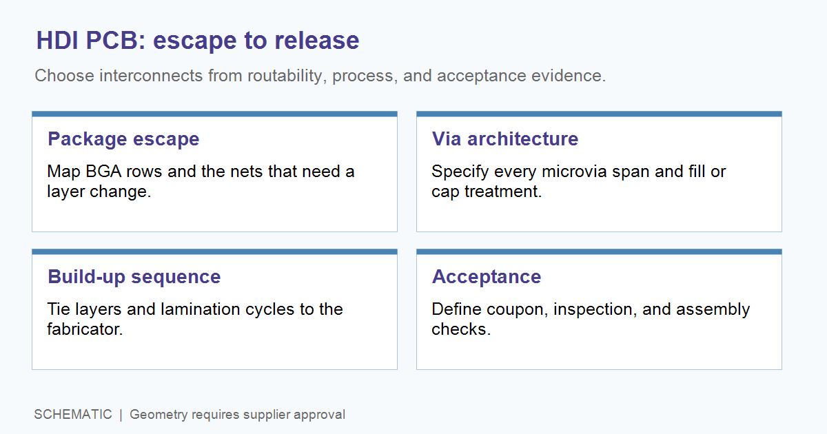
Table of Conent
Table of Conent
An HDI PCB should be specified from the package escape problem backward, not from a preferred microvia count. First map the BGA lands and nets that must leave each row, then check the actual pad, trace, spacing, and reference-plane geometry against a fabricator-approved stackup. Only after that should the team choose through vias, selective blind microvias, via-in-pad, or a sequential build-up structure. The released package must state every via span, fill and cap treatment, layer sequence, acceptance method, and assembly condition. BGA pitch alone cannot prove that an HDI build is needed or that a given build-up will route.
This approach matters to both engineering and purchasing. A board may pass a top-layer routing check yet require an unquoted lamination cycle, an unsupported laser-drill geometry, or an unreliable stacked interface. The goal is a controlled route from BGA escape to manufacturable bare board and inspectable assembled product.
Does the BGA really require HDI?
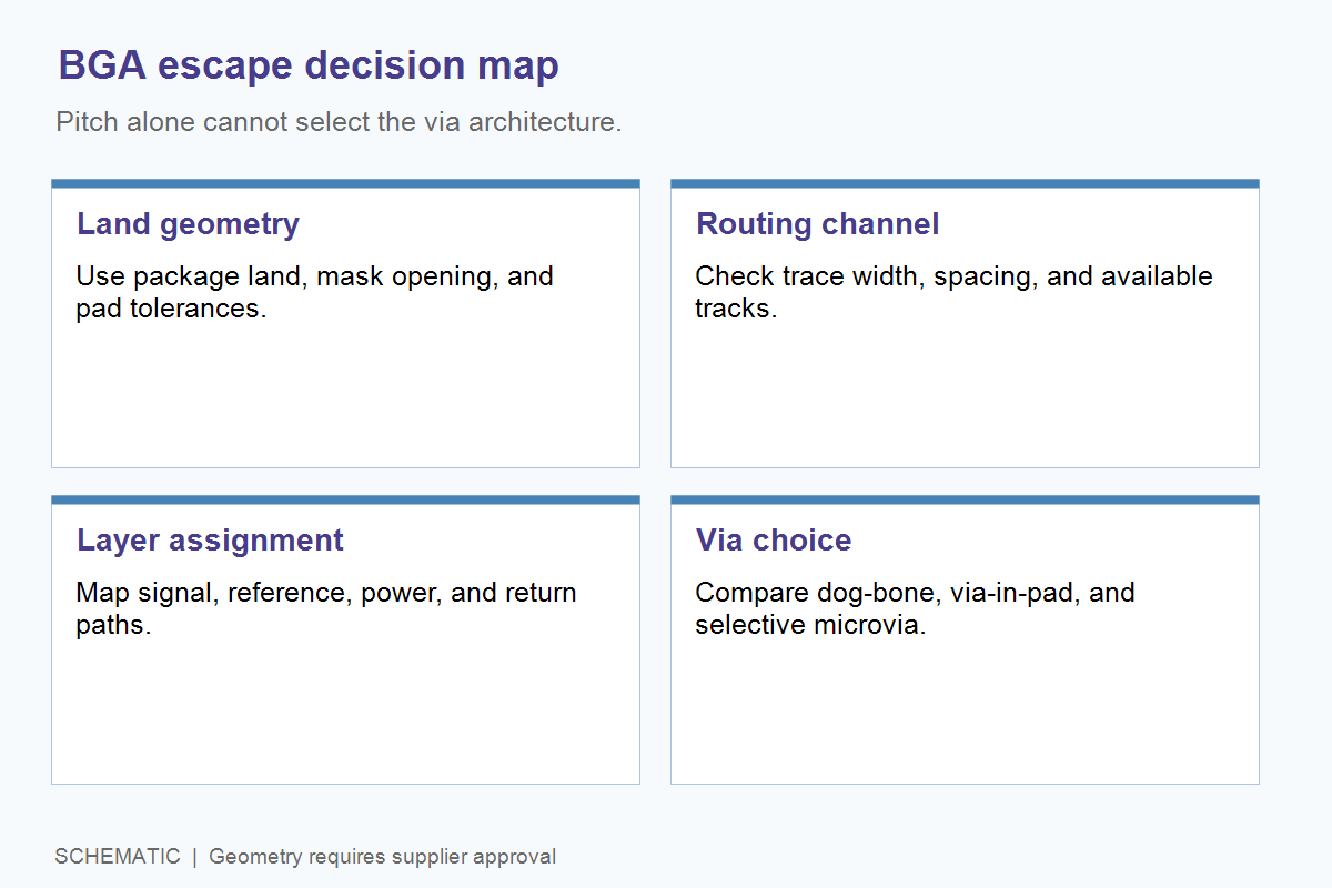
Prove that conventional routing cannot meet the electrical and mechanical requirements before adding HDI complexity. The practical inputs are package land diameter and pitch, solder-mask definition, the signal and power pin map, allowed trace width and spacing, copper thickness, reference-plane needs, through-via land size, and board outline. The number of signal rows that must escape on each layer depends on all of them, not only on pitch.
Start with a small escape study rather than routing the whole board. Mark which outer rows can leave on the component layer, which nets can move through a conventional via outside the land field, and which inner rows have no legal channel. Then assign critical power, ground, and high-speed nets to appropriate layers. A dog-bone fanout may be sufficient for part of the package, while a selective microvia solves only the blocked rows. Texas Instruments’ BGA package guide explicitly uses trace/space, via type, and routing between capture pads to estimate layer needs; its example dimensions describe that package study, not a universal factory rule.
The via-in-pad release guide explains the local pad-treatment decision. HDI release is broader: it also defines via layer spans, build-up sequence, registration, material, and acceptance evidence. The 10-layer stackup guide provides a conventional multilayer comparison so a team can test whether additional ordinary routing layers are preferable to a more complex via build.
Which via and layer structure is buildable?
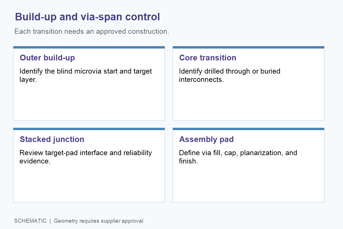
Define each interconnect as a start layer, target layer, finished geometry, and fabrication process. “Microvia” alone does not tell a supplier whether the hole is blind, stacked, staggered, filled, plated shut, or placed in a solderable land. Similarly, a 1+N+1 or 2+N+2 shorthand does not replace a layer drawing that identifies dielectric thickness, core transitions, and lamination sequence.
For each proposed structure, ask the fabricator to approve laser-drill diameter and depth, capture and target pads, annular ring, minimum dielectric, copper thickness, registration, fill method, and any stacked interface. Do not transfer a generic online capability table into the CAD rules. Supplier-specific process windows and the actual material construction control whether a nominal geometry can be built with margin.
| Option | Use when | Release and RFQ question |
|---|---|---|
| Conventional through via and dog-bone | Legal channels exist outside the BGA lands | Do capture pads consume required escape space on deeper layers? |
| Selective blind microvia | Only certain rows need an adjacent-layer transition | Which exact nets and layer spans require laser drilling? |
| Filled, capped via-in-pad | A via must occupy a solderable land | What fill, cap, planarization, and inspection keep the pad solderable? |
| Additional build-up or stacked transitions | Approved routing still cannot reach required layers | What lamination sequence, interface design, and reliability evidence are required? |
The first quotation should compare structures against the same BGA escape and electrical constraints. If the package study shows a few blocked rows, send the pin map, preliminary stackup, and proposed via spans for an interconnect and assembly review before committing to a full sequential build-up. The review can identify which features need supplier approval and which remain conventional.
How should microvia reliability change the decision?
Where a design depends on stacked or otherwise demanding microvia structures, specify acceptance evidence suited to the product risk. IPC has warned that some microvia-to-target-pad failures can remain latent through bare-board acceptance and emerge after reflow, environmental stress, or service. That warning does not mean every microvia design will fail. It means a room-temperature continuity pass or a single conventional microsection may not prove the required reliability for a high-performance product.
Ask the product owner and qualified fabricator whether representative via-chain coupons, thermal-stress testing, electrical resistance monitoring, cross-sections, or other approved methods are required. Define which production panel, via span, stacked interface, and process revision the sample represents. The acceptance plan should distinguish prototype learning, first-article qualification, routine lot control, and failure investigation. IPC’s published warning is useful context; the exact test method and acceptance limits must come from the applicable specification and agreed qualification plan.
A staggered construction may avoid some stacked junctions, but it can consume more routing area. A stacked path may free space yet require stronger process control. Evaluate both using a supplier-approved design and the actual product risk. The 12-layer PCB guide introduces the broader stackup and via trade-offs; this article’s release matrix translates those choices into supplier and buyer questions.
How do fabrication and assembly constraints meet?
Finish the escape study at the assembled pad, not at the drill file. A via opening in a BGA land can draw solder away or create a poor joint if its treatment is unsuitable. Fill, copper cap, planarization, surface finish, solder-mask opening, stencil design, reflow profile, and inspection access need a common assumption. TI’s package guide discusses solder wicking from larger open via holes; the magnitude and suitable remedy depend on the actual pad and process.
Also check whether the BGA’s power and high-speed paths retain continuous reference and return structures as they move between layers. A routable fine trace is not automatically acceptable for impedance, current, heat, or test access. Do not trade a blocked escape for a broken return plane or an untestable assembly. The PCB lamination guide shows why material, dielectric thickness, copper distribution, and press sequence must agree in a multilayer release.
What belongs in the HDI release package?
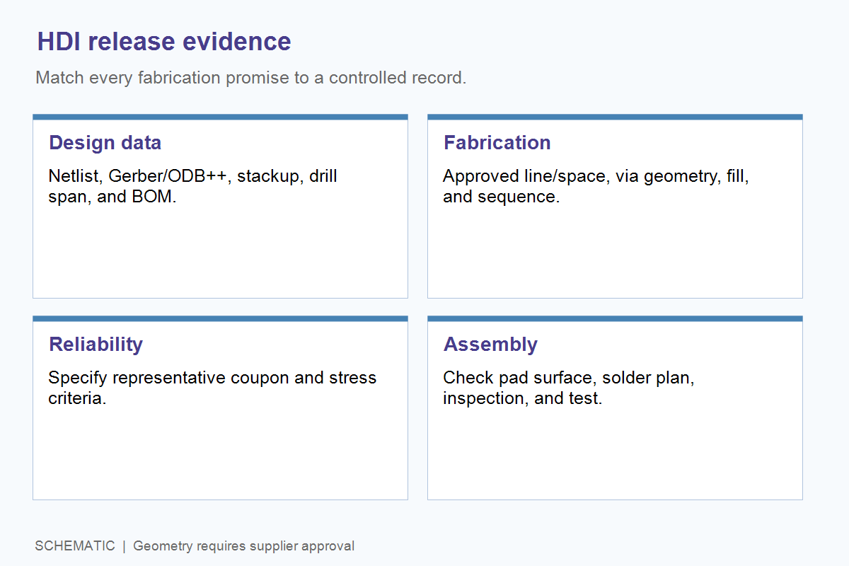
A complete package lets the fabricator quote a specific construction and lets the assembler understand the pad and test assumptions. Provide a controlled layer stackup, BGA pin/land map, netlist, Gerber or ODB++ data, drill files separated by via span, fabrication drawing, material and finish requirements, via fill/cap definition, impedance requirements where applicable, and a revisioned BOM and assembly drawing. Record any permitted material or via substitutions and who may approve them.
The release matrix below connects the design decision to evidence. It is a scope checklist, not a claim that every project needs every test.
Before a purchase order, reconcile the fabrication drawing against the generated drill outputs: the layer-span names, via counts, and pad-treatment notes should describe the same revision. Keep supplier questions and approved answers with that revision. This prevents a CAM clarification from silently changing the interconnect that the escape study and reliability plan evaluated.
| Controlled decision | Files or specification | Evidence to agree before order |
|---|---|---|
| BGA escape | Package drawing, pin map, escape study, trace/space and pad rules | Supplier DFM approval of the actual geometry |
| Build-up | Layer stack, material family, dielectric targets, lamination sequence | Approved construction and revision |
| Via spans | Separate drill data, start/target layers, pad and fill/cap rules | Fabrication inspection and representative coupon plan if needed |
| Assembly interface | Land pattern, finish, mask, stencil and placement data | Solderability and hidden-joint inspection scope |
| Electrical acceptance | Netlist, impedance or test requirements, reporting format | Agreed bare-board and assembled-board test records |
The HDI PCB manufacturing page is the relevant commercial starting point, but a project-specific capability check still needs the exact stackup and via architecture. Do not describe a build as approved merely because a broad HDI service page exists.
What is the practical release decision?
Choose the simplest supplier-approved interconnect that routes the package while preserving electrical performance and an adequate reliability plan. Freeze the BGA escape geometry, via spans, build-up, and acceptance evidence together; changing any one of them after quotation can change cost, lead time, and qualification scope. A selective microvia may solve a local density problem, while a larger build-up is justified only when the complete routing study needs it.
For a full PCB assembly project, send the stackup, BGA package and escape map, drill-span data, Gerbers or ODB++, BOM, placement files, quantities, and inspection requirements with the released fabrication and assembly package. That gives engineering one set of assumptions for bare-board fabrication, component sourcing, solderable BGA pads, inspection, and quotation.
Technical references
IPC design standards overview (accessed October 20, 2026); IPC microvia reliability warning (accessed October 20, 2026); Texas Instruments Flip Chip Ball Grid Array Package Reference Guide (accessed October 20, 2026). Apply current project specifications and supplier-approved limits to the actual construction.
Latest Blog



Contact Info
Phone: +86-755-82882936
Email: [email protected]
WhatsApp: +86-13570802455
Wechat: +86-13570802455
Address: 2nd floor,D Bldg.,Electric Link Technology Bldg.,Gongming,Guangming New Dist.,518106 Shenzhen, China