
PCB Board Assembly Explained: Process, Components, and Quality Control
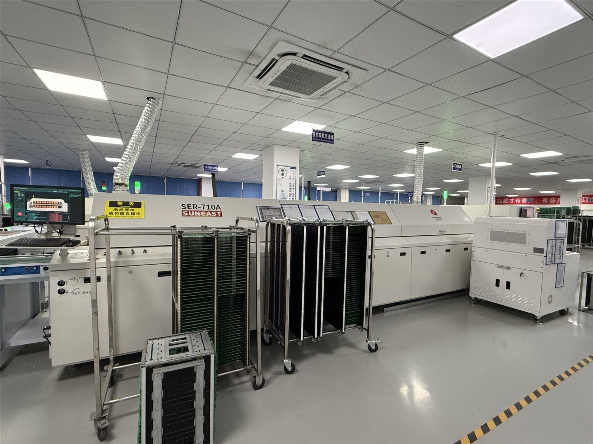
Table of Conent
Table of Conent
A bare printed circuit board becomes a functional electronic product only after components are mounted, soldered, inspected, and tested. That transformation is the PCB board assembly process. For an OEM buyer, understanding the process is useful for more than technical curiosity. Each assembly step creates specific cost, schedule, quality, and reliability risks that should be addressed before production begins.
This guide explains how an assembly PCB board moves from manufacturing data to a tested PCBA. It also covers the components involved, the quality controls that matter, and the evidence a capable supplier should provide. The goal is to help engineering and procurement teams define requirements clearly and evaluate a printed circuit board assembly manufacturer on measurable production capability rather than price alone.
What Is PCB Board Assembly?
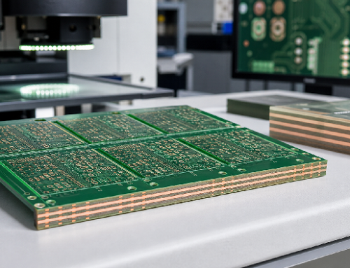
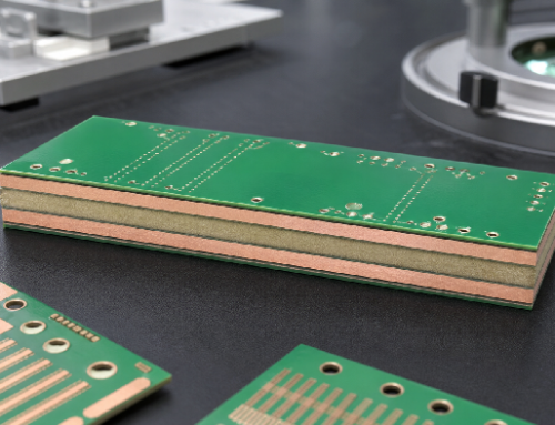
PCB board assembly is the process of attaching electronic components to a fabricated printed circuit board and verifying that the resulting assembly performs as intended. The bare PCB provides the conductive paths, insulation, pads, holes, and mechanical structure. The assembly operation adds resistors, capacitors, integrated circuits, connectors, sensors, power devices, and other parts to create a functional circuit.
The terms PCB assembly, circuit board assembly, and printed circuit board assembly are often used interchangeably. PCBA usually refers to the completed or partly completed assembled board, while PCB refers to the unpopulated board. This distinction matters when requesting quotations because PCB fabrication and component assembly use different materials, equipment, lead times, and quality controls. For a concise comparison, see PCB vs. PCBA.
The Main Components in a Printed Circuit Board Assembly
A reliable assembly starts with a controlled bill of materials and a design that matches the intended manufacturing process. Most PCBAs contain several component groups.
Passive components
Resistors, capacitors, and inductors shape signals, set operating points, filter noise, and store energy. They are available in very small surface-mount packages as well as larger through-hole formats. Package selection affects placement speed, solder-joint geometry, inspection access, and rework difficulty.
Semiconductors
Microcontrollers, processors, memory devices, diodes, transistors, voltage regulators, and power modules perform the active functions of the circuit. Fine-pitch packages such as QFNs, BGAs, and CSPs require accurate paste deposition, stable placement, controlled reflow, and inspection methods that can evaluate joints hidden beneath the package.
Electromechanical parts
Connectors, switches, relays, transformers, displays, and mechanical hardware often experience physical load or repeated use. Their footprint design, anchoring, solder volume, and insertion process should reflect those stresses.
The bare PCB and solder materials
The PCB itself is a critical assembly input. Surface finish, solder-mask registration, pad geometry, flatness, moisture condition, and cleanliness all influence solderability. Solder paste combines metal alloy powder with flux and is normally deposited through an SMT stencil. Flux activity, paste storage, thawing time, stencil condition, and print parameters must be controlled as part of the process.
PCB Assembly Process: From Data Review to Finished PCBA
Although every product has different requirements, a controlled printed circuit board PCB assembly generally follows the steps below.
1. Manufacturing data and DFM review
Before material is released, the manufacturer reviews the Gerber or ODB++ data, centroid or pick-and-place file, bill of materials, assembly drawings, approved vendor list, test requirements, and revision status. A design-for-manufacturing review checks component spacing, polarity markings, pad design, tooling rails, fiducials, panelization, thermal balance, and test access.
This review should produce actionable questions rather than silent assumptions. If the BOM calls for an unavailable component, the supplier should not substitute a part without written approval. If the centroid data conflicts with the drawing, the revision mismatch should be resolved before programming the line. Buyers can reduce delays by sending a complete package; the article on documents required for PCB assembly provides a practical checklist.
2. Incoming material inspection and traceability
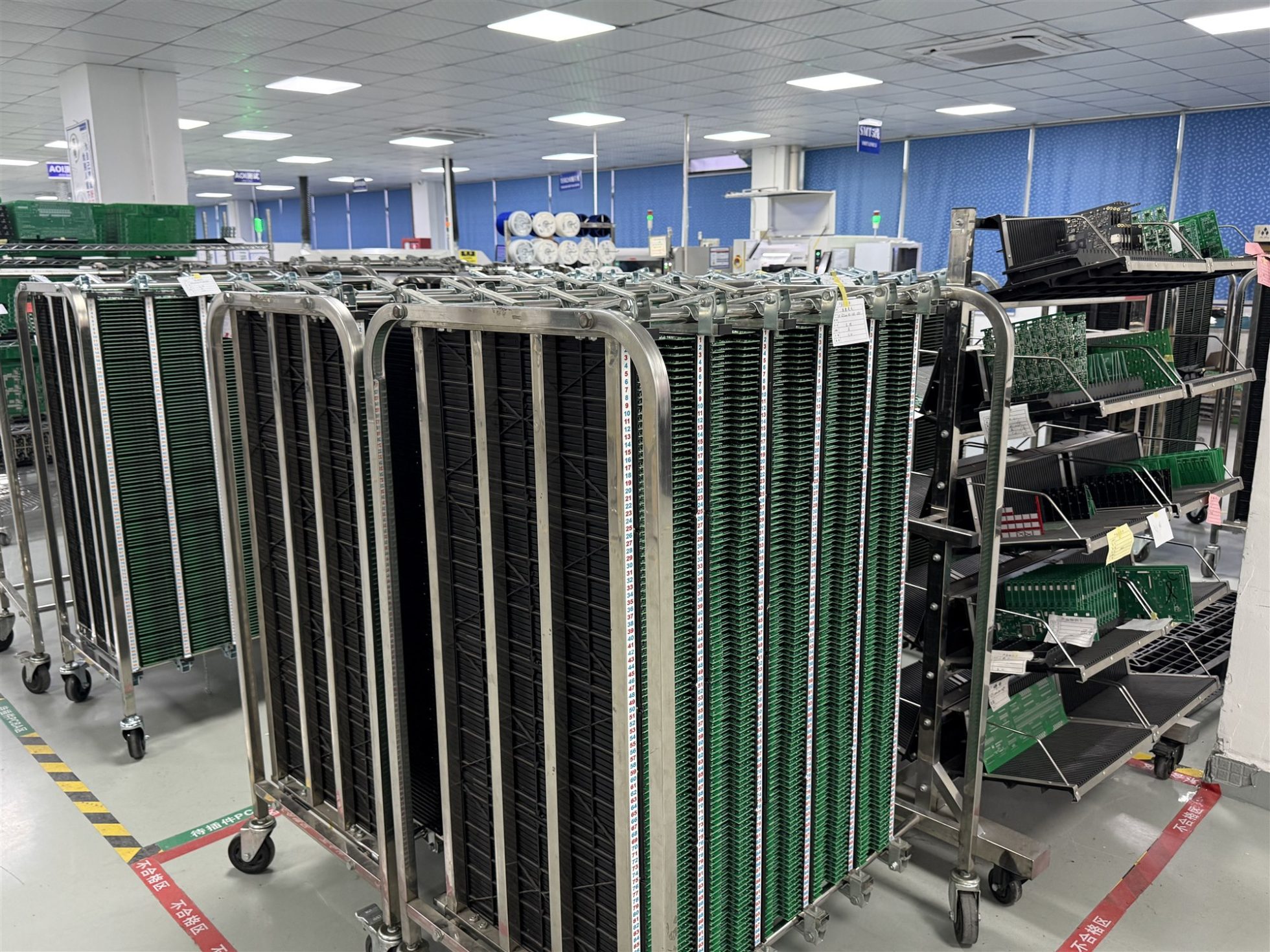
The manufacturer receives bare boards, electronic components, solder materials, and mechanical parts. Incoming inspection may verify part numbers, quantities, date codes, packaging condition, moisture-sensitivity labels, PCB dimensions, surface finish, solderability, and certificates. High-risk or counterfeit-sensitive parts may require enhanced inspection or electrical testing.
Traceability connects each production lot to its PCB batch, component lots, material dates, line records, inspection results, and operators or equipment. This becomes especially important during failure analysis. A date code printed on a package is not a complete traceability system unless it is linked to the finished assembly lot.
3. Solder paste printing and SPI
A stencil printer transfers solder paste onto the SMT pads. Paste volume and alignment have a direct effect on opens, shorts, solder balls, voiding, and insufficient joints. The team controls stencil alignment, squeegee pressure and speed, separation settings, underside cleaning, paste condition, and environmental limits.
Solder paste inspection, or SPI, measures deposit height, area, volume, and offset. Because many downstream solder defects begin at printing, SPI provides early process feedback. Trend data is more valuable than a simple pass/fail result because it can show gradual stencil blockage or print drift before defects escape.
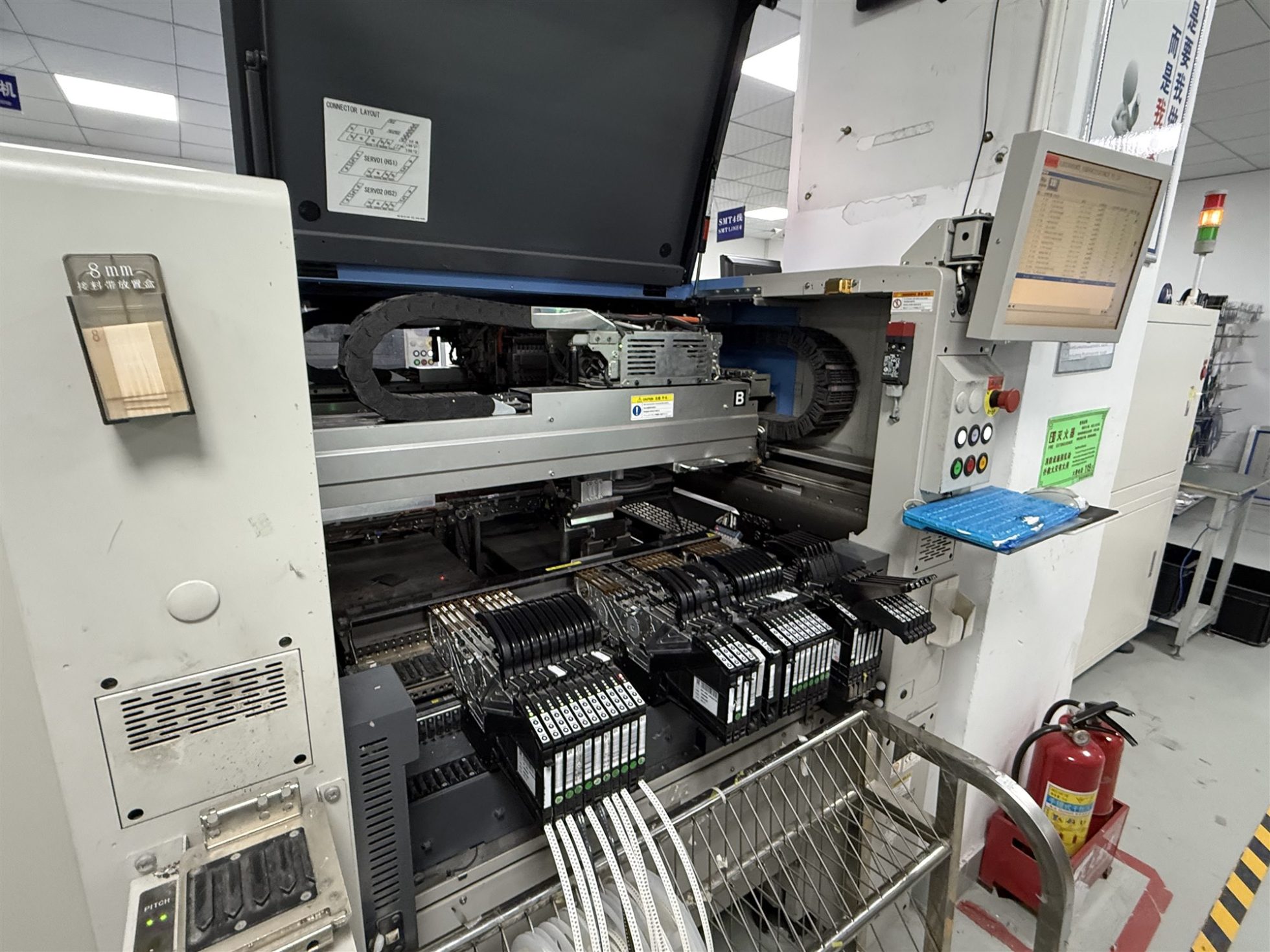
4. Automated component placement
Pick-and-place machines identify components from feeders and position them on the pasted PCB. Machine programs define coordinates, rotation, package data, nozzle selection, and vision parameters. First-article verification should confirm polarity, orientation, reference designators, and component values before the full lot proceeds.
Placement accuracy alone does not guarantee correctness. Feeder loading must be independently checked, and line clearance should prevent parts from a previous build remaining on the machine. For low-volume, prototype, or mixed-technology work, see AssyPCB’s PCB prototype assembly capabilities.
5. Reflow soldering
The populated board passes through a reflow oven with controlled heating, soak, peak, and cooling zones. The thermal profile must activate the flux, melt the alloy, wet the surfaces, and cool the joints without damaging parts or the laminate. Large thermal masses, BGAs, small passives, and temperature-sensitive components can make one profile difficult to optimize.
A manufacturer should profile the actual product or a representative assembly rather than relying only on an oven recipe. Thermocouples placed at critical locations show whether every joint remains within the solder paste and component limits. The detailed guide to reflow soldering explains this stage further.
6. Through-hole insertion and soldering
Components that require mechanical strength, high current capacity, or a package not suited to SMT may be inserted through plated holes. Depending on volume and layout, soldering may use wave, selective, pin-in-paste, robotic, or manual methods. A mixed-technology assembly often completes SMT first and through-hole work afterward.
Through-hole quality depends on hole-to-lead clearance, flux application, preheat, solder contact time, alloy condition, and barrel fill. Heavy connectors may also need fixtures or mechanical fasteners. AssyPCB’s THT PCB assembly page describes the available service.
7. Cleaning, coating, and final mechanical work
Cleaning requirements depend on flux chemistry, product environment, process qualification, and customer specifications. “No-clean” flux does not automatically mean residues are acceptable for every high-voltage, high-impedance, medical, automotive, or harsh-environment application. Ionic contamination criteria should be defined where reliability demands it.
Optional operations include conformal coating, underfill, staking, heat-sink installation, cable attachment, enclosure assembly, labeling, depanelization, and programming. Each operation should have its own workmanship and inspection criteria.
Quality Control Throughout Circuit Board Assembly
Quality should be built into the process rather than inspected only at the end. A capable supplier combines prevention, in-process feedback, final inspection, and functional evidence.
First-article inspection
The first completed unit or panel is checked against the BOM, drawings, polarity requirements, component values, and workmanship standard. Production should not continue until discrepancies are resolved. For repeat builds, the first article also confirms that approved revisions and machine programs were loaded.
Automated optical inspection
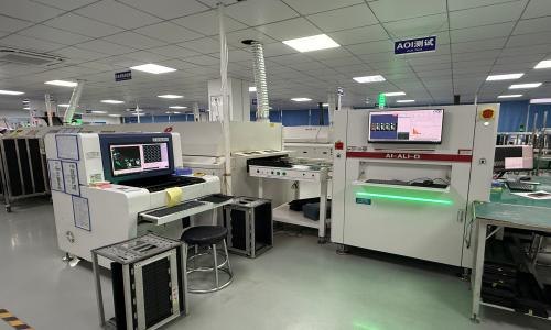
AOI uses programmed cameras and lighting to identify missing, shifted, reversed, tombstoned, or visibly defective components and solder joints. It offers fast, repeatable coverage but must be programmed and reviewed by trained personnel. Excessive false calls can hide real trends, while insufficient thresholds can miss defects. Learn more in the guide to automated optical inspection testing.
X-ray inspection
X-ray inspection is important for BGAs, bottom-terminated components, power packages, and other hidden joints. It can reveal bridging, insufficient solder, opens, head-in-pillow conditions, voiding, and alignment problems. Buyers should define sampling or 100% inspection requirements based on product risk instead of assuming every assembly receives X-ray inspection.
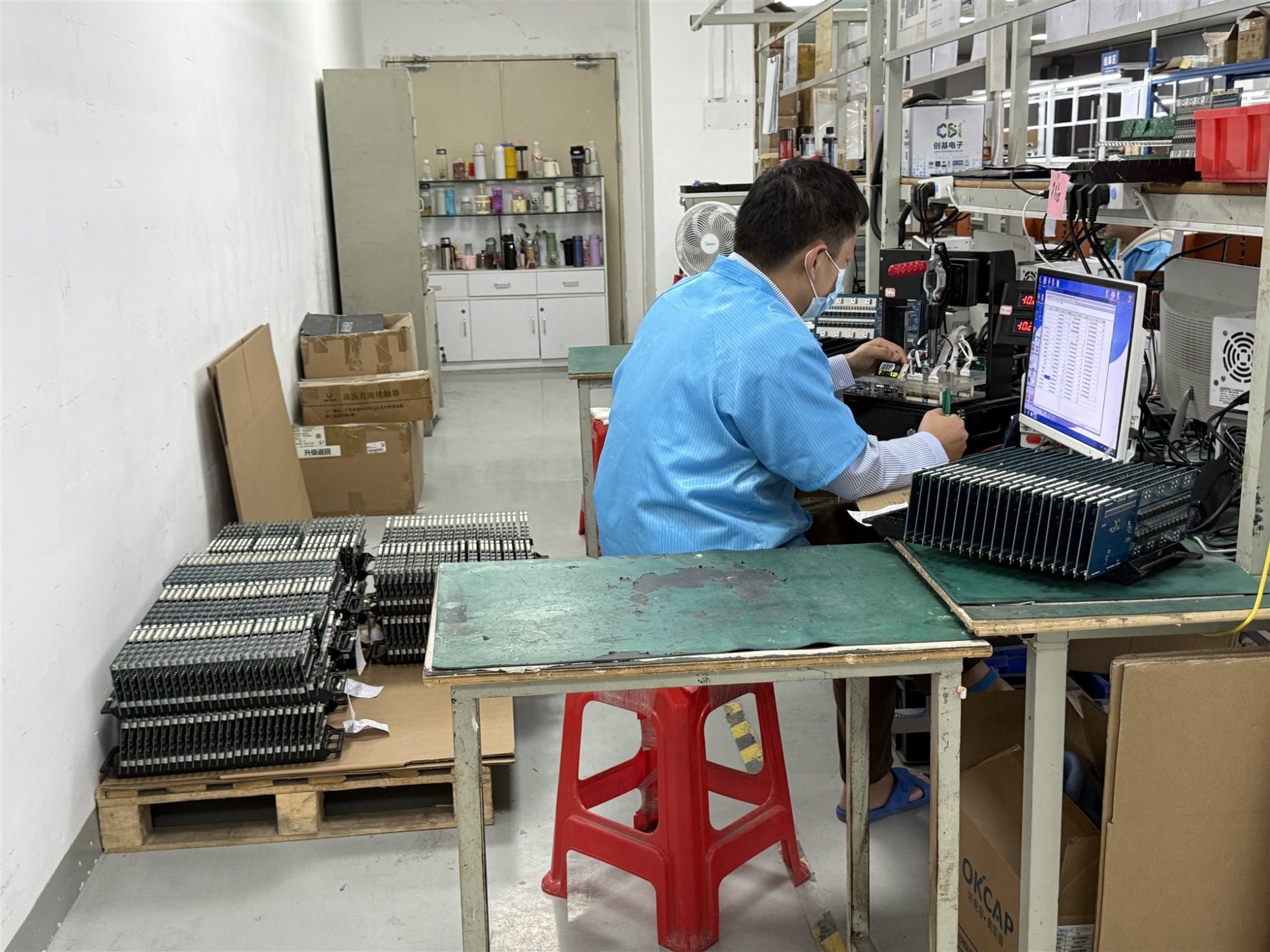
Electrical and functional testing
Automated inspection shows how the assembly looks; electrical testing shows whether connections and functions behave correctly. In-circuit testing can measure components and check nets. Flying-probe testing offers flexible coverage for lower volumes without a dedicated fixture. Functional testing powers the assembly and verifies specified inputs, outputs, communications, loads, and operating modes.
A test requirement should state limits, test sequence, firmware version, fixture ownership, data retention, and failure handling. “Functional test required” is too vague for a dependable quotation. The PCBA testing process guide outlines common methods and their tradeoffs.
Workmanship standards and process metrics
Many contracts reference IPC-A-610 for electronic assembly acceptability and J-STD-001 for soldered electrical and electronic assemblies. The applicable class, revision, customer drawings, and approved deviations should be stated in the purchase documentation. A standard reference does not replace product-specific requirements.
Useful production metrics include first-pass yield, defect rate by process, rework rate, test yield, and recurring defect Pareto data. Ask how the supplier controls nonconforming material, performs root-cause analysis, approves repairs, and closes corrective actions. A low shipment defect rate is meaningful only when supported by stable inspection and test coverage.
How to Prepare an Assembly PCB Board for Quotation
A complete RFQ reduces assumptions and makes supplier comparisons more accurate. Provide the following information:
- Gerber, ODB++, or IPC-2581 fabrication and assembly data
- Bill of materials with manufacturer part numbers and approved alternates
- Centroid or pick-and-place file
- Assembly drawings with polarity and special workmanship notes
- PCB fabrication specification and panel requirements
- Required quantity, forecast, target schedule, and acceptable split deliveries
- Programming files and controlled firmware revision
- Inspection, electrical test, functional test, and reporting requirements
- Applicable IPC class, regulatory requirements, and material restrictions
- Packaging, labeling, serialization, and traceability requirements
Clarify whether the supplier will purchase all materials, use customer-supplied parts, or support a mixed model. A turnkey PCB assembly service can simplify procurement, but the agreement should define alternate-part approval, excess material, attrition, and ownership.
How to Evaluate a PCB Assembly Manufacturer
The right supplier must match the product’s technology, volume, regulatory environment, and risk level. During evaluation, ask for evidence in six areas.
- Technical fit: Confirm package sizes, BGA capability, board dimensions, mixed technology, materials, coating, programming, and test coverage.
- Process control: Review stencil control, SPI, first-article approval, thermal profiling, AOI, X-ray, ESD controls, and calibration.
- Supply-chain control: Understand approved sources, counterfeit avoidance, substitution approval, moisture-sensitive handling, and material traceability.
- Quality system: Check certifications relevant to the product and examine nonconformance, corrective-action, document-control, and change-control practices.
- Communication: Define response times, engineering-query handling, production reporting, escalation paths, and time-zone coverage.
- Total cost: Compare tooling, NRE, component pricing, attrition, test fixtures, freight, lead time, yield risk, and rework terms rather than unit price alone.
Before committing a major order, use a prototype or pilot build to validate data, fixtures, process assumptions, inspection criteria, and communication. Review the build report and defects together. The lessons should be incorporated into controlled documentation before volume production.
Common PCB Board Assembly Defects and Their Causes
Typical defects include solder bridges, opens, insufficient solder, tombstoned passives, component shift, reversed polarity, wrong parts, damaged pads, through-hole fill problems, and contamination. These symptoms often have multiple possible causes. For example, an open joint may result from insufficient paste, coplanarity, oxidation, placement error, warpage, or an unsuitable thermal profile.
Effective corrective action therefore goes beyond repairing the failed unit. It contains the affected lot, verifies inspection coverage, identifies the physical and systemic causes, changes the process or documentation, and checks whether the action prevents recurrence. Detailed examples are covered in PCB assembly problems and solutions.
Final Takeaway
PCB board assembly is a connected manufacturing system, not a single soldering operation. Accurate data, controlled materials, stable printing and placement, verified thermal processes, appropriate inspection, and product-specific testing all contribute to the reliability of the finished PCBA. Buyers get better results when requirements are measurable, revisions are controlled, and supplier decisions are based on documented capability.
For projects that also require an experienced independent PCB and PCBA manufacturing partner, visit ORINEW PCB to review additional fabrication and assembly capabilities.
Latest Blog
Contact Info
Phone: +86-755-82882936
Email: [email protected]
WhatsApp: +86-13570802455
Wechat: +86-13570802455
Address: 2nd floor,D Bldg.,Electric Link Technology Bldg.,Gongming,Guangming New Dist.,518106 Shenzhen, China