
Capacitor Values 103: Design, Selection, and PCB Application Guide
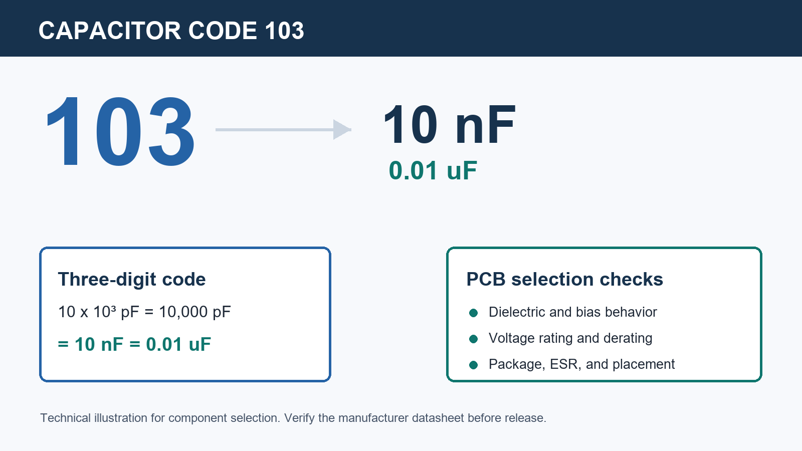
Table of Conent
Table of Conent
A capacitor marked 103 has a nominal capacitance of 10 nF, which is also written as 0.01 uF or 10,000 pF. That conversion answers the immediate identification question, but it is not enough to release a BOM. In a PCB design, the dielectric, DC-bias behavior, voltage rating, tolerance, package, ESR, ESL, and placement determine whether a 103 capacitor performs as intended.
This guide explains how to decode capacitor value 103 and how to turn that value into a defensible component selection for decoupling, timing, filtering, and signal-conditioning circuits.
What does capacitor code 103 mean?
The three-digit code is expressed in picofarads. The first two digits are the significant figures and the last digit is the number of zeros to add:
10 x 103 pF = 10,000 pF = 10 nF = 0.01 uF
For example, a marking of 104 represents 100,000 pF, or 100 nF. A marking of 102 represents 1,000 pF, or 1 nF. The code identifies nominal capacitance, not voltage rating, dielectric material, tolerance, temperature characteristic, or package. Those fields must come from the full manufacturer part number and datasheet.
Where a 10 nF capacitor is used
A 10 nF capacitor is common because it fits several frequency ranges and circuit functions. The correct use depends on impedance, bias conditions, and the rest of the network.
- High-frequency bypassing: A 10 nF ceramic capacitor can supplement larger local decoupling capacitors near a fast IC power pin. Its usefulness depends heavily on loop inductance and package size.
- RC timing and reset networks: With a specified resistor, 10 nF can establish a delay or filter brief transitions. Tolerance, leakage, and input threshold characteristics define the actual timing window.
- Signal filtering: In an RC low-pass network, 10 nF may suppress high-frequency noise. Calculate the cutoff from the selected resistor and then check source impedance, load impedance, and signal rise time.
- EMI and transient control: A 10 nF capacitor may be part of a snubber, common-mode path, or input filter. Safety class, pulse energy, and failure mode matter when the capacitor connects to hazardous voltages or a line interface.
Do not assume that every 10 nF part is interchangeable. A C0G/NP0 10 nF capacitor, an X7R 10 nF capacitor, and a film capacitor with the same nominal value have different stability, loss, available voltage ratings, and mechanical behavior.
Choose the dielectric for the circuit requirement
For ceramic multilayer capacitors, the dielectric class is often the first selection decision after the nominal value. It controls value stability against temperature, voltage, and time.
C0G/NP0 for stable analog or timing functions
C0G/NP0 capacitors have very stable capacitance and low loss compared with high-permittivity ceramics. They are appropriate when the capacitance directly affects frequency, timing, gain, or filter accuracy. Their available capacitance and package options may be more limited, and they can cost more than X7R parts.
X7R for general-purpose decoupling and filtering
X7R is widely used for bypassing and general filtering because it offers useful capacitance in compact packages. Its actual capacitance changes with applied DC voltage, temperature, and aging. For a 10 nF part the loss may be modest in many applications, but the datasheet curve is still the governing evidence. Use the capacitance-versus-DC-bias graph for the exact case size and voltage rating.
Y5V and similar dielectrics need explicit limits
High-permittivity dielectrics can provide small, inexpensive parts, but their capacitance can vary substantially with temperature and bias. They are generally unsuitable when the circuit needs predictable capacitance. Do not substitute them into a timing, precision filter, or qualification-controlled design without an engineering review.
Set a voltage rating with margin, then verify DC-bias behavior
Capacitor voltage rating is not merely a compliance field. A higher voltage-rated MLCC of the same nominal capacitance may retain more capacitance under DC bias because its construction and dielectric thickness differ. The direction and magnitude must be confirmed from the manufacturer data for the exact part.
Start with the maximum steady-state voltage, then include expected rail tolerance, startup overshoot, switching spikes, and environmental conditions. For a 5 V rail, selecting a 6.3 V part may meet a basic rating requirement but leave little operating margin. A 16 V or 25 V option can be justified where bias stability, surge exposure, or reliability requirements call for it. That is a design decision, not a universal rule.
For circuits that see repetitive pulses, calculate the transient condition rather than relying on the DC rail value. Consider the capacitor’s permitted ripple current, dissipation factor, temperature rise, and the relevant safety or automotive requirements. Data unavailable in the component datasheet should be treated as a sourcing or engineering question, not assumed favorable.
Select the package with layout parasitics in mind
A 10 nF value can be supplied in packages ranging from very small chip sizes to larger MLCCs, film parts, and through-hole styles. Package choice affects assembly yield, working voltage, mechanical stress sensitivity, and high-frequency performance.
- ESL and placement: Small packages and short, wide connections can reduce inductance, which matters for high-frequency bypassing. Place the capacitor close to the power and ground connection it serves, with a compact current loop.
- Assembly and inspection: Use a land pattern consistent with the component manufacturer’s recommendation and your assembly process. Overly large pads, board flexure, or poor panel handling can crack MLCCs.
- Voltage and availability: A small package may not offer the required voltage rating or qualified source options. Evaluate approved alternates before locking the BOM.
- Mechanical environment: If vibration, depaneling, connector loading, or thermal cycling is significant, consider soft-termination MLCCs, placement away from board edges, or a more suitable capacitor technology.
For board material and stackup decisions that affect impedance and return paths, review the requirements for an FR4 PCB build alongside the component placement rules. A capacitor’s benefit can be lost when its return path is long or discontinuous.
Use a 103 capacitor correctly in common circuits
Decoupling a digital IC
A 10 nF capacitor is often used with one or more larger capacitors to cover a broader impedance range. The component value alone does not guarantee low rail impedance. Confirm the power-distribution network, capacitor placement, via arrangement, package inductance, and the IC vendor’s recommendations. Avoid placing the capacitor on the other side of a plane split or routing the power path through a long trace before it reaches the pin.
Creating an RC low-pass filter
For a first-order RC low-pass filter, the nominal cutoff frequency is:
fc = 1 / (2 pi R C)
With 10 nF and 1 kOhm, the nominal cutoff is about 15.9 kHz. Real behavior also depends on resistor tolerance, capacitor tolerance, capacitor dielectric, source impedance, load impedance, and parasitic capacitance. State the permitted frequency range in the design documentation rather than quoting only the nominal result.
Using a capacitor in a reset or timing path
When a 10 nF capacitor sets reset delay or oscillator timing, C0G/NP0 may be more appropriate than a high-permittivity MLCC if tolerance across temperature and voltage is tight. Check the input leakage and threshold behavior of the device being controlled. A nominal RC calculation does not represent a guaranteed reset interval unless all relevant limits are included.
When you are preparing a prototype build, submit the Gerber files, BOM, pick-and-place data, required quantity, and test requirements through the PCB quotation form. An engineering and quotation review can identify package, assembly, sourcing, and documentation questions before production release.
BOM and DFM checklist for a 10 nF capacitor
Before releasing the design, use a component record that is specific enough for purchasing and assembly to identify the intended part. At minimum, review the following:
- Nominal capacitance: 10 nF, 0.01 uF, or 10,000 pF.
- Dielectric and temperature characteristic, such as C0G/NP0 or X7R.
- Capacitance tolerance and its effect on the circuit limit.
- Rated voltage, operating voltage, expected transient voltage, and the manufacturer’s DC-bias curve when applicable.
- Package, termination option, land pattern, and approved manufacturer part number.
- Assembly constraints, including MSL where relevant, reflow profile, board flex risk, and inspection requirements.
- Lifecycle status, authorized sources, and qualified alternates with the same functional requirements.
The site’s capacitor component overview can help frame the technology choice, but the component datasheet remains the authority for a production part number. For builds that include component sourcing and assembly, the turnkey PCB assembly service is the relevant commercial path.
Conclusion
Capacitor code 103 means 10 nF, or 0.01 uF. The right 10 nF capacitor is selected by more than that marking: match the dielectric to the stability requirement, set voltage margin using real operating conditions, check bias and temperature behavior, and choose a package and placement that fit the electrical and manufacturing constraints. Document those choices in the BOM so a nominal-value substitution does not change the circuit in production.
For a build review, send the Gerber files, BOM, fabrication requirements, assembly quantity, and test expectations through the engineering contact page. The review can clarify manufacturability, component sourcing, and quotation inputs before the order is placed.
Latest Blog
Contact Info
Phone: +86-755-82882936
Email: [email protected]
WhatsApp: +86-13570802455
Wechat: +86-13570802455
Address: 2nd floor,D Bldg.,Electric Link Technology Bldg.,Gongming,Guangming New Dist.,518106 Shenzhen, China