
Clamping Diode: Design, Selection, and PCB Application Guide
Table of Conent
Table of Conent
A clamping diode protects a circuit by providing a controlled current path when a transient pushes a node beyond its intended voltage range. The part may be a TVS diode, a zener diode, a Schottky diode, or another diode arrangement, depending on the fault and the protected device. The critical selection question is not simply whether a diode has a suitable nominal voltage. It is whether the complete circuit keeps the protected pin below its maximum limit while safely handling the expected transient current and energy.
For PCB designers and NPI teams, that decision connects component data, cable and source conditions, layout parasitics, assembly constraints, and the BOM. This guide provides a practical way to select and place a clamping diode without treating a catalog voltage value as a complete protection design.
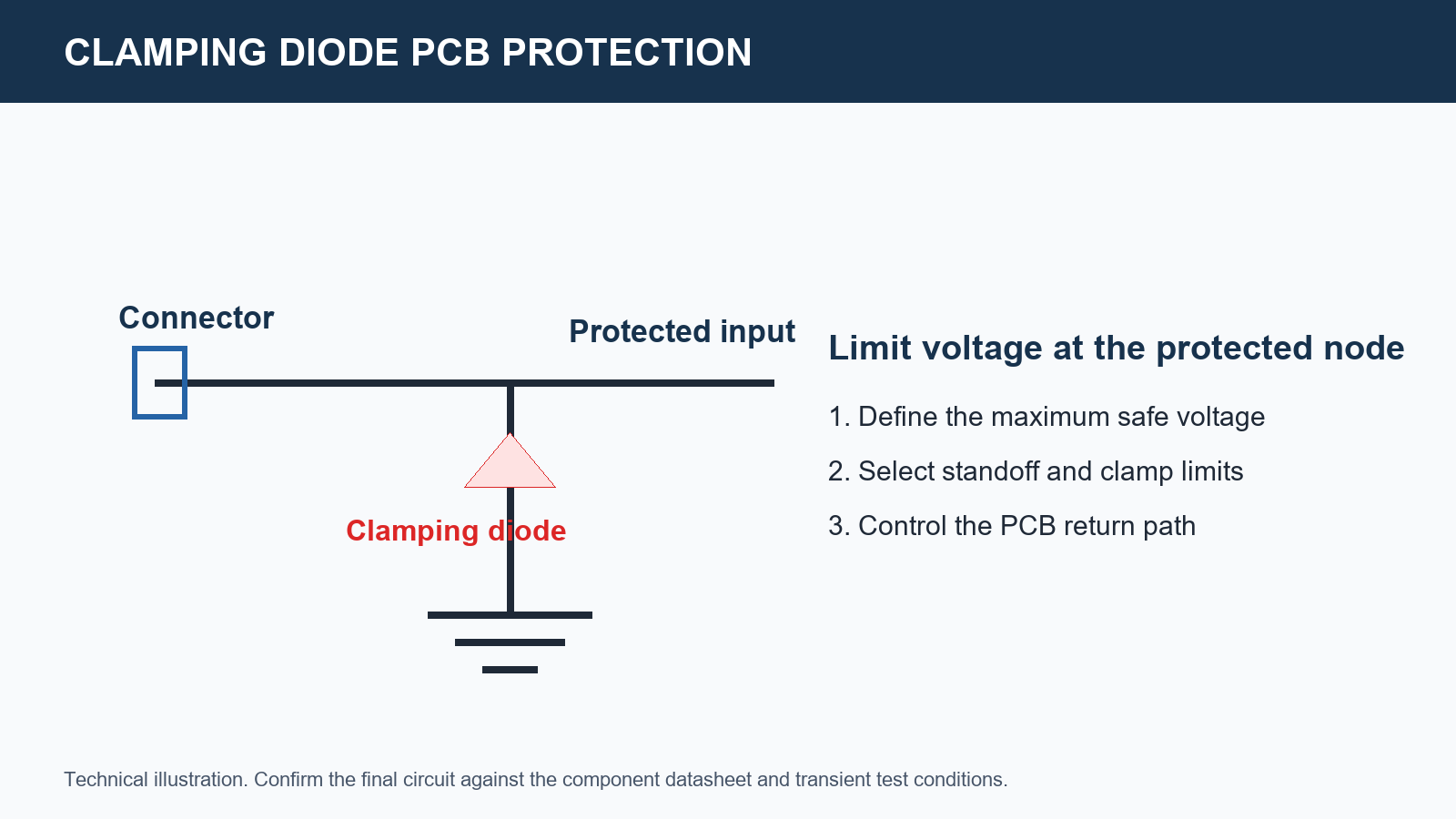
How a clamping diode works
In normal operation, a shunt clamping diode is selected so that it does not conduct significantly at the maximum expected working voltage. When the node rises above the diode’s breakdown or forward-conduction region, current is diverted away from the protected circuit. The voltage at the protected node is then determined by the diode’s current-voltage characteristic, the source impedance, the wiring and trace inductance, and the return-path impedance.
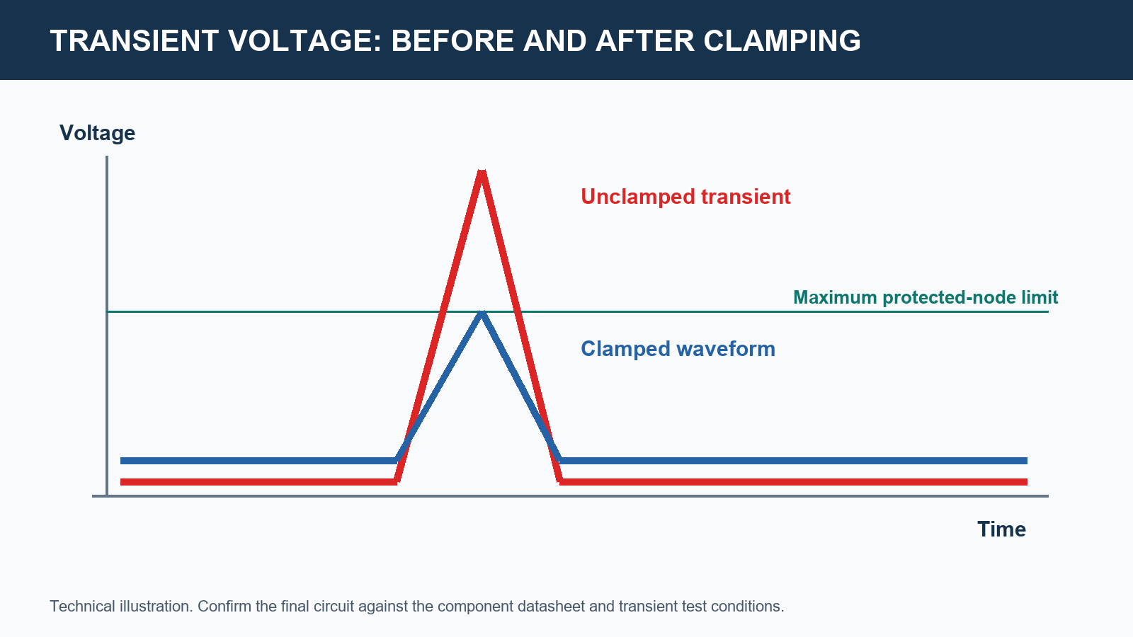
That last point matters. A datasheet clamping-voltage figure is usually specified at a stated pulse current and with a defined test waveform. It is not a universal maximum for every installation. A longer cable, a different surge waveform, or a high-inductance ground path can produce a higher local voltage at the IC than the simple schematic suggests.
Start with the protected device and the transient
Write down the maximum voltage that the receiving IC, converter, connector, or transistor can tolerate at the protected node. Use the absolute maximum rating only as a survival limit, not automatically as a recommended operating condition. If the device vendor specifies a preferred clamp level or an IEC test condition, use that as the design requirement.
Next, define the threat. A 24 V industrial input, a USB data line, a relay coil, and a reverse-connected battery input do not present the same event. Record the normal voltage range, expected overshoot, source impedance, repetition rate, pulse duration, cable environment, and applicable test standard. If the transient waveform is not available, label that gap in the project risk log and obtain it before qualification.
Separate standoff voltage, breakdown voltage, and clamping voltage
These terms are related but not interchangeable. The reverse standoff voltage is the level at which a TVS diode is intended to remain off within its specified leakage range. Breakdown voltage is the region where the part begins to conduct a defined test current. Clamping voltage is measured at a higher stated pulse current. A part with a standoff voltage above the normal rail can still clamp too high for a sensitive IC when the surge current reaches its datasheet test level.
Use the maximum values in the relevant columns, not only typical values. Then include margin for supply tolerance, load dump or switching behavior where applicable, temperature, and layout overshoot. A diode that passes a bench test with a short probe ground lead may not protect the same node in the finished product.
Choose the diode topology for the failure mode
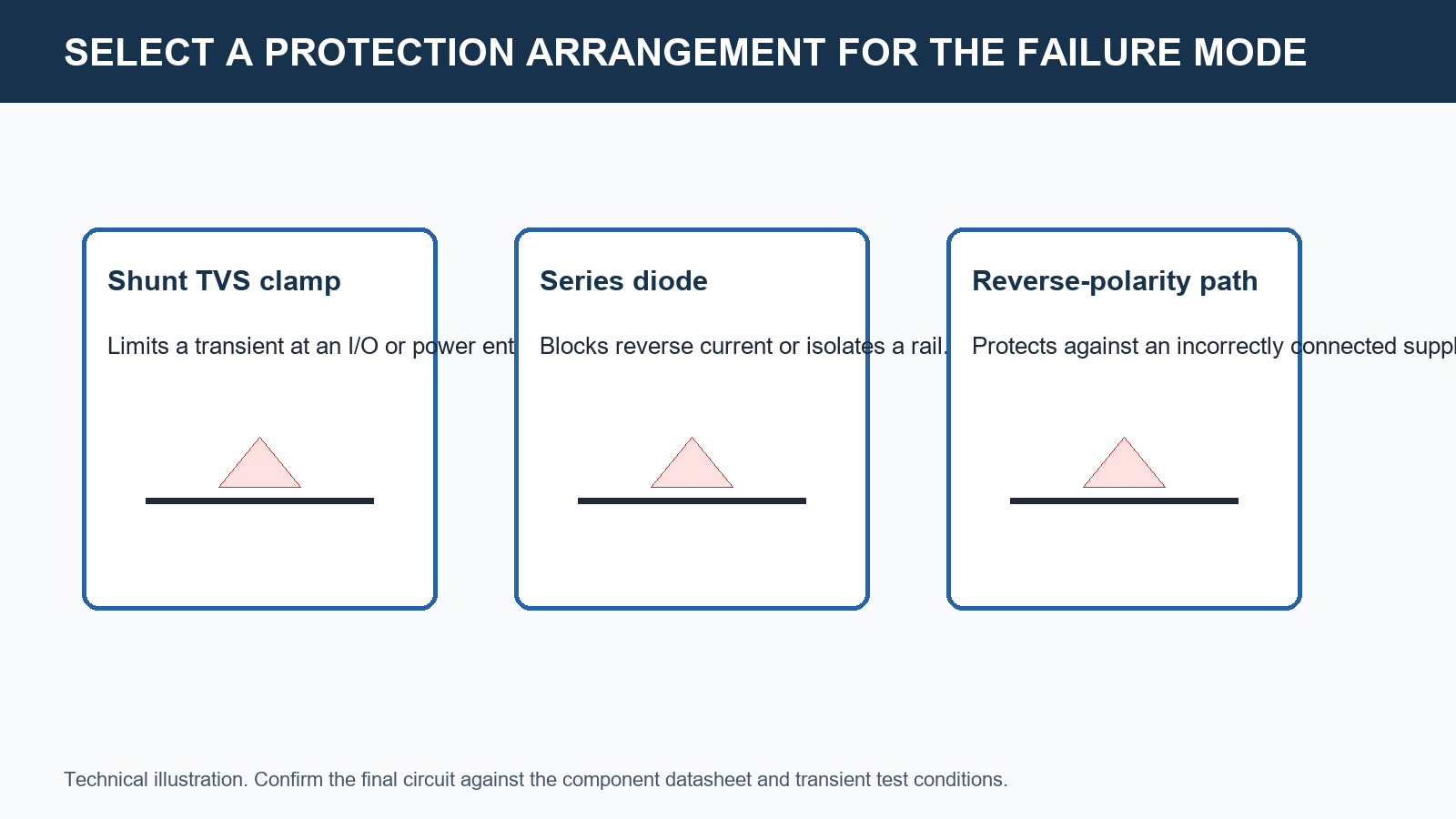
A shunt TVS diode is often appropriate for an external power or signal entry where the goal is to divert transient current to a reference plane. A series diode is more suitable when reverse current blocking or supply isolation is the objective. A diode to a local rail can protect a low-voltage signal only if that rail can absorb or redirect the injected current without rising beyond another component’s limit. The topology must include the destination of the surge current, not just the symbol placed near the connector.
For a broader review of diode functions and other components in the circuit, see the basic electronic component functions. If the circuit also includes rectification, the choice of a rectifier diode arrangement affects the normal and fault voltages that the protection network will see.
Check surge current, energy, and repetition
Peak pulse power ratings are useful only when their test waveform matches, or conservatively bounds, the intended event. Compare the data sheet’s pulse width, waveform, and duty conditions with the actual surge. Repeated pulses can heat the junction even when a single-pulse calculation appears acceptable. For a relay, solenoid, or inductive load, calculate the stored energy and determine where it is dissipated after turn-off.
Do not use package size as a proxy for surge capability. Confirm the manufacturer’s rating, derating curve, thermal conditions, and any board-area assumptions. Include the upstream protection elements, such as fuses, current-limiting resistors, PTCs, or series impedance, in the analysis. They may reduce current into the clamp, but only when their response at the relevant time scale is known.
When an input filter is part of the protection path, verify the input filtering considerations together with the clamp. A filter capacitor or inductor can alter peak current, ringing, and the voltage applied to the diode.
Do not ignore capacitance on data and high-speed signals
TVS and other clamp parts add capacitance. On slow DC inputs that may be unimportant. On RF, high-speed serial, precision analog, or high-impedance sensing lines, it can change bandwidth, attenuation, rise time, and signal integrity. Select a low-capacitance device when the interface requires it, and compare the capacitance at the actual reverse voltage and frequency where the datasheet provides that information.
Also examine leakage current. At elevated temperature, leakage can create offset error in high-impedance circuits or interfere with a weak pull-up. A component that is acceptable for an automotive supply line can be unsuitable for a low-level sensor input even if both use the same nominal clamping voltage.
PCB placement determines the real clamp performance
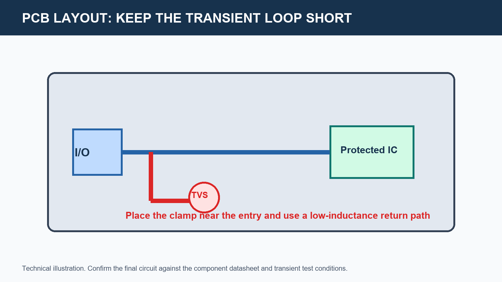
Place the shunt clamp close to the point where the transient enters the board. Route the incoming path to the clamp before routing it toward the protected IC. Use a short, wide connection from the clamp to the reference plane or return conductor. The transient loop includes the connector, diode, return path, and source. Reducing that loop inductance helps reduce the voltage added by fast current change.
Avoid routing the surge current through a sensitive analog return, narrow thermal-relief connection, or long trace shared with the protected device. Keep the protected trace on the IC side of the clamp. Where a connector has multiple pins, make the intended return path explicit in the stackup and layout review. The FR4 PCB stackup and return-path requirements should support the current path rather than leave it to an assumed plane connection.
Preparing a prototype or pilot build? Submit the Gerber files, BOM, connector and cable details, required quantity, and transient or test requirements through the PCB quotation form. An engineering and quotation review can identify component, assembly, and documentation questions before the design is released.
BOM and DFM checklist
- State the protected-node maximum voltage and the normal operating range.
- Record standoff voltage, maximum breakdown range, and clamping voltage at the relevant current.
- Identify the transient waveform, peak current, duration, repetition, and test method.
- Check junction temperature, power derating, and the effect of upstream series impedance.
- Specify package, polarity or bidirectional configuration, land pattern, and approved manufacturer part number.
- For signal lines, document capacitance and leakage limits.
- Review placement, return current, board flex risk, and inspection access.
- Qualify alternates against the complete limit set, not only nominal voltage.
For projects that need component sourcing and assembly as part of the same release, the turnkey PCB assembly service is the relevant commercial path. Provide the approved part number, alternates policy, assembly drawings, and test expectations with the BOM.
Common clamping-diode design mistakes
A frequent mistake is choosing a part from its headline power rating without comparing the test waveform to the actual event. A 600 W rating at a short standardized pulse does not establish suitability for a longer pulse, a repeated inductive event, or a surge with low source impedance. Another mistake is selecting a standoff voltage close to the nominal supply and overlooking production tolerance, cold-crank behavior, charger behavior, or switching overshoot. The result can be leakage or unintended conduction during normal operation.
Layout can create an equally serious failure. Placing the diode near the protected IC rather than the connector lets transient current travel along the board before it is diverted. A long ground route can add enough inductive voltage to defeat an otherwise suitable clamp. Treat the placement review as part of the electrical design. On a multilayer board, identify the entering conductor, the diode pads, the return plane or conductor, and the protected trace in one review view.
Finally, avoid approving substitutes using only the nominal reverse-voltage field. An alternate may have a different maximum clamp voltage, capacitance, leakage limit, dynamic resistance, package thermal path, or polarity. Those differences can affect both protection and normal circuit behavior. State the critical limits in the approved-alternate policy so purchasing and manufacturing do not infer interchangeability from a broad component description.
Plan verification before design release
Verification should represent the installed circuit, not only the diode in isolation. Define the test injection point, source impedance, pulse shape, supply state, operating temperature, and measurement bandwidth. Probe the voltage at the protected pin with a technique that does not introduce a long ground lead or obscure fast overshoot. Record both the peak protected-node voltage and the recovery behavior after the event.
For example, an external cable interface may need ESD, EFT, surge, or switching-transient tests appropriate to its intended environment. The relevant standard and performance criteria are project requirements; they cannot be inferred from the diode part number. Test the production-intent layout and connector configuration, including any external cable or power supply that changes the source impedance. Inspect the diode and adjacent PCB area after testing for damage, discoloration, solder cracking, or value drift.
Close the review by linking the schematic reference designator, BOM line, layout location, test report, and approved alternate list. That traceability makes it possible to re-evaluate the protection network when a connector, cable, IC, board stackup, or sourcing option changes.
Conclusion
A clamping diode works only when the component, transient, current path, and protected device are evaluated as one system. Choose the diode from maximum working voltage, clamp voltage at real current, energy and repetition limits, capacitance and leakage, then give it a short low-inductance PCB return path. Document those constraints in the BOM and layout notes so the protection design survives sourcing and manufacturing changes.
For an engineering review before release, send the Gerber files, BOM, operating voltage range, interface details, and test requirements through the engineering contact page. The review can clarify manufacturability, sourcing, and quotation inputs for the build.
Latest Blog


Contact Info
Phone: +86-755-82882936
Email: [email protected]
WhatsApp: +86-13570802455
Wechat: +86-13570802455
Address: 2nd floor,D Bldg.,Electric Link Technology Bldg.,Gongming,Guangming New Dist.,518106 Shenzhen, China