
IPC-9121: A Practical Guide to PCB Fabrication Troubleshooting

Table of Conent
Table of Conent
IPC-9121 helps engineers investigate problems in printed circuit board fabrication. Its practical value is the connection between an observed defect, possible process causes, and evidence that can support a corrective action. For an OEM or purchasing team, the most useful question is not simply whether a supplier owns the handbook. It is whether the supplier can explain a problem with traceable observations and demonstrate that the proposed fix worked.
This guide explains the role of IPC-9121 and offers an original investigation workflow for designers and buyers. It does not reproduce the handbook’s defect tables or set numerical acceptance limits. Use the applicable licensed standards, fabrication drawing, and agreed purchasing requirements for contractual decisions.
What IPC-9121 covers
IPC’s official IPC-9121A scope and contents identify the document as a reference for investigating fabrication problems, their potential causes, and corrective actions. The public contents span design documentation, imaging, lamination, drilling, plating, and other production stages. The February 2022 Revision A is the edition represented by that public preview; confirm the edition applicable to your project rather than relying on a blog’s revision claim.
The handbook can help organize a technical conversation, but reading a possible cause is only the beginning. A visible condition may have several explanations. The investigation must connect the specific board, material lot, process stage, and inspection evidence before selecting a correction.
IPC-9121, IPC-A-600, and IPC-6012 have different roles
These documents answer different questions. IPC-9121 supports fabrication troubleshooting. IPC-A-600 illustrates observable printed-board conditions and their acceptability. IPC-6012 addresses qualification and performance requirements for rigid printed boards. IPC explains the relationship between workmanship interpretation and performance requirements on its printed-board standards overview.
For an order, identify the applicable revision, product class, drawing requirements, and agreed exceptions. A troubleshooting reference should not become a substitute for the purchase specification. Likewise, a supplier’s use of a handbook does not establish company certification or prove that every delivered board meets your requirements.
Start with a problem statement that can be checked
“The boards are unreliable” is too broad to investigate efficiently. A useful statement names the observed condition, its location, the affected revision and lot, and when it appeared. Record whether the issue was found during bare-board inspection, after assembly, or during a defined test. If it appeared after heating, preserve the temperature profile and handling history rather than assuming fabrication is the only possible source.
Keep observations separate from explanations. “Three measured holes fall below the drawing’s finished-hole tolerance” is an observation. “The plating line caused undersized holes” is a hypothesis until records and measurements support it. This distinction makes communication more productive and helps avoid unnecessary changes to a stable process.
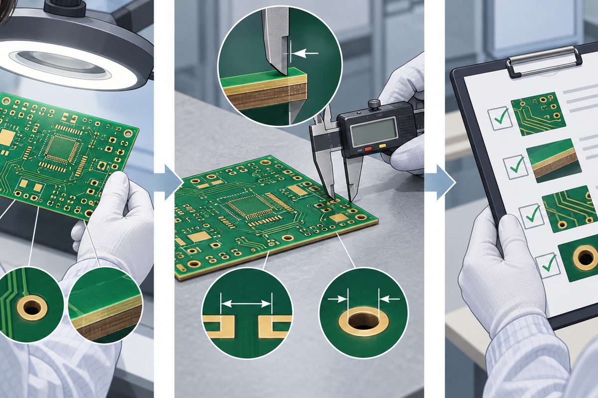
A practical investigation sequence
1. Contain the suspect material
Identify affected lots and segregate them while the issue is evaluated. Preserve representative suspect boards, comparison samples, packaging, and labels. Avoid cleaning, reworking, or sectioning every sample before the investigation team agrees on a plan. Altering the evidence can make it harder to distinguish a production defect from later damage.
2. Establish the comparison
Compare the observation with the controlled drawing and purchase specification. Confirm that the inspector used the correct units, revision, and measurement method. A confusing layer map or inconsistent drill note can produce a dispute that looks like a factory failure. For multilayer projects, review the multilayer PCB design and release requirements alongside the actual production data.
3. Map where the condition could originate
Trace the affected feature through the manufacturing route. A conductor dimension involves artwork, imaging, and etching; a hole condition involves drilling and subsequent preparation or plating; a layer-bonding concern requires a different record set. The point is to narrow the review to plausible stages without declaring a cause prematurely.
4. Gather evidence that distinguishes hypotheses
Ask what each proposed test would establish. Surface observation, dimensional measurement, electrical test, and microsection analysis reveal different things. Select the method appropriate to the condition and agree on sample selection. A measurement that cannot distinguish competing explanations may add delay without resolving the problem.
5. Verify the correction and prevention
Define success before running the trial. Compare the result against the same requirement that established the original problem, then check whether the change introduced another issue. Assign an owner for the production control, documentation update, and follow-up review. Replacing a shipment resolves the immediate shortage; demonstrating effective control addresses recurrence.
Turn common symptoms into better questions
The following examples are investigation prompts, not diagnoses or copied IPC defect entries. Each requires evidence tied to the affected product.
- Unexpected conductor width: Is the difference uniform across a panel or localized? Which artwork revision was used, and at what process stage was the dimension measured?
- Layer registration concerns: Is the mismatch consistent with a tooling offset, or does it vary with panel position? Can the supplier compare alignment data with the intended stackup and drill targets?
- Suspected bonding defects: What does inspection actually show, and when was the condition first observed? Review material identity, handling, and the relevant production records before attributing it to a press setting.
- Electrical opens or shorts: Which nets and coordinates fail, and do comparison boards show the same pattern? Confirm the test data matches the released design before investigating the physical feature.
For a bonding investigation, understanding the relationship between cores, prepreg, copper distribution, and dielectric spacing helps you ask more precise questions. Our PCB lamination and process-control guide explains those design inputs.
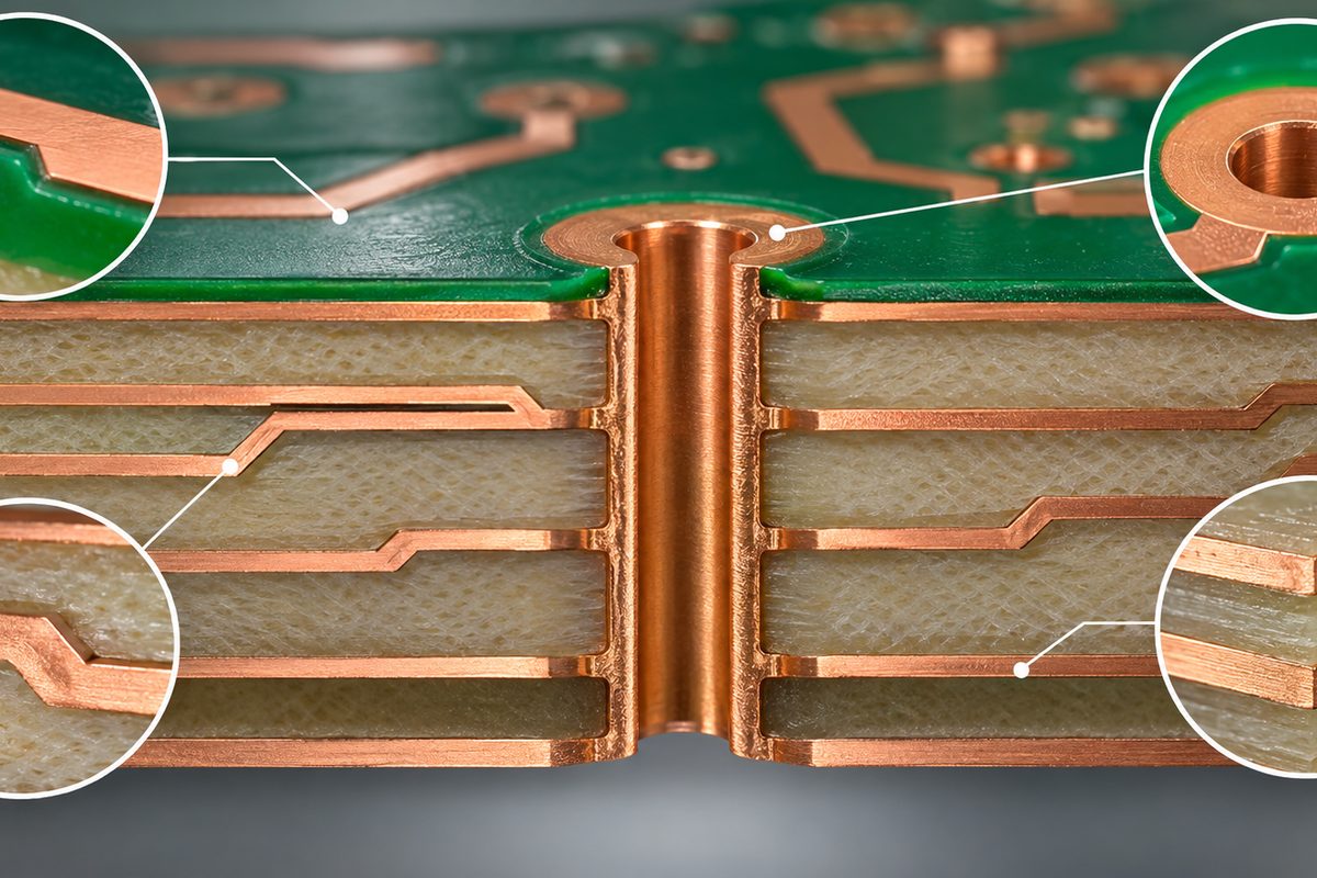
Prepare a supplier evidence package
A concise package is easier to act on than a long email chain with unidentified photographs. Include the board part number, revision, purchase order, lot identifiers, and a short factual description. Add an annotated location image with a scale where useful, the applicable requirement, the measurement method, and the number of affected units relative to the number examined.
Provide relevant released files and explain any later assembly or test exposure. If the reported condition depends on a thermal cycle, describe that cycle and whether comparison samples experienced it. Keep sensitive design data in the agreed sharing channel and identify which files the supplier may use for analysis.
Preparing a new build with demanding inspection requirements? Submit the fabrication data, stackup, applicable specifications, quantity, and requested inspection records through the PCB engineering and quotation request. Those inputs allow the requirements and manufacturing scope to be reviewed before the order is released.
Prevent repeat problems during the next design release
Many useful corrective actions belong in the release package. Make finished dimensions and tolerances explicit, identify material restrictions, and reconcile the stackup with the layer files. Label controlled-impedance requirements clearly and resolve conflicting notes before production. If a supplier proposes a construction change, record its approval and update the relevant documentation.
Do not add a tight tolerance merely because a previous job had a problem. Ask whether it is functionally necessary, measurable, and compatible with the selected process. Excessively restrictive or ambiguous notes can increase cost and review time without improving the product. Review the PCB manufacturing capabilities against your actual design requirements and request clarification where a feature needs special consideration.
For the next RFQ, submit Gerber or ODB++ data, drill files, the fabrication drawing, and any acceptance or documentation requirements through the fabrication quote form. Identify unresolved questions so the engineering review can address them before price and production assumptions are finalized.
Evaluate a corrective-action response
A useful response shows the observed condition, the supporting evidence, and the relationship between the cause and the correction. Look for clear scope: which lots were reviewed, what material was contained, and how the supplier determined whether other work was affected. Where uncertainty remains, the response should name it and explain what additional evidence is needed.
Ask for verification results that address the original failure mechanism. A passing electrical test alone does not answer every mechanical or structural question. Conversely, an attractive surface photograph does not prove electrical connectivity. The required evidence should follow the product requirement and the investigation question, not the convenience of the available equipment.
Check that the preventive action has a defined owner and an implementation date. A work instruction, incoming-material check, or equipment control is useful only if it is maintained and checked. Request a follow-up plan proportionate to the problem, including how recurrence will be recognized and what triggers another review.
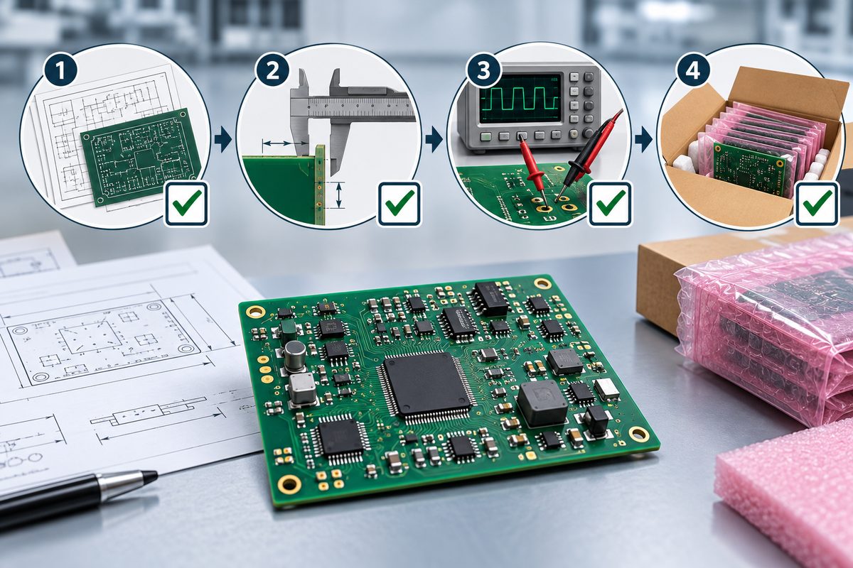
Conclusion
IPC-9121 provides a reference point for fabrication troubleshooting, while a successful investigation depends on controlled requirements and product-specific evidence. Define the problem precisely, preserve samples, test the plausible causes, and verify the correction. For buyers, those habits make supplier discussions more useful and help convert a defect report into a practical prevention plan.
Starting a new fabrication project? Send the released files, quantity, schedule, and inspection expectations through the online PCB RFQ form for an engineering and quotation review. Include any lessons from earlier builds so the next release can address them explicitly.
Latest Blog
Contact Info
Phone: +86-755-82882936
Email: [email protected]
WhatsApp: +86-13570802455
Wechat: +86-13570802455
Address: 2nd floor,D Bldg.,Electric Link Technology Bldg.,Gongming,Guangming New Dist.,518106 Shenzhen, China