
MIL-STD-1553 PCB Grounding: Manage Isolation Returns and EMI
Table of Conent
Table of Conent
MIL-STD-1553 PCB grounding is not a choice between “one ground” and “split grounds.” The layout must preserve the intended transformer isolation, line-interface return currents, logic and power integrity, shield or chassis strategy, creepage and clearance, and electromagnetic compatibility of the installed equipment. Treat the connector, coupling network, transformer, transceiver, power conversion, reference planes, enclosure, and cable as one current-path system.
A useful design review begins with the exact terminal architecture and applicable program requirements. Document whether the interface is direct or transformer coupled, which transformer ratios and transceiver circuit apply, where high transmit currents return, how shields and chassis are bonded, and which equipment-level environmental and EMI categories must be verified. A generic “1553-compliant PCB” statement is not enough evidence.
Define the 1553 terminal architecture first
Map each redundant channel from the controller or FPGA through the transceiver, isolation transformer, any coupling transformer or network, protection components, connector, stub, and installed harness. Identify the data-bus return paths, logic grounds, power returns, chassis or case connections, cable shields, and any galvanically isolated domains.
Do not infer the required transformer or coupling circuit from another board. Manufacturer documentation and the applicable MIL-STD-1553 program specification should define turns ratios, center-tap connections, supply rails, receive and transmit interfaces, and component values. Holt and Data Device Corporation publish transceivers, transformers, and reference information with different integrations and supply requirements.
| Design area | Question to close | Release evidence |
|---|---|---|
| Bus coupling | Is the terminal direct or transformer coupled? | Schematic, transformer identity, and connector map |
| Transmit return | Where does the pulsed line-driver current return? | Current-path review and copper geometry |
| Isolation boundary | Which nets, planes, shields, and protection parts cross it? | Isolation diagram and spacing rules |
| Chassis and shield | Where are cable shields and case returns bonded? | Installation and mechanical drawing |
| EMI verification | Which equipment configuration and categories apply? | Approved test plan and configuration record |
Keep transformer behavior tied to the PCB layout
Isolation and coupling transformers are part of the physical layer, not generic magnetic components. Review turns ratio, winding configuration, droop, overshoot, common-mode behavior, insulation, package, temperature range, and the exact approved part number. A compatible footprint alone does not establish electrical equivalence.
DDC’s published MIL-STD-1553 technical FAQ advises locating transformers close to the board connector and keeping appropriate planes away from transformers and analog bus traces because added capacitance can affect terminal impedance. It also calls attention to the substantial transmit current in the transformer center-tap return. Apply the current device manufacturer’s circuit rather than copying numeric guidance to a different architecture.
Keep transformer-to-connector routing short and physically separated from clocks, switching nodes, high-current converters, and unrelated fast interfaces. Route the paired conductors with consistent geometry and avoid branches that create uncontrolled coupling. Preserve creepage and clearance around the transformer and isolation boundary according to the approved electrical and environmental requirements.
Design the transmit-current return deliberately
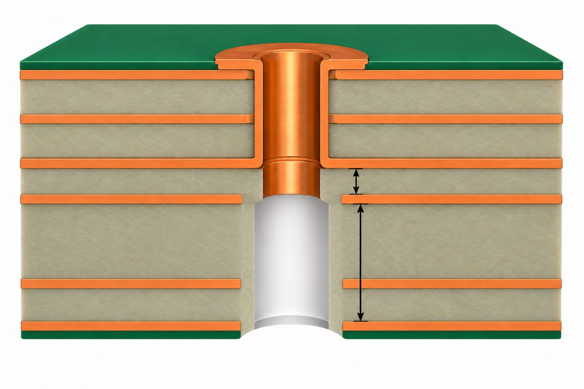
The line driver can create large, fast current pulses compared with ordinary logic loads. Give the specified transformer center-tap or driver return a short, low-impedance path to the intended supply return. Avoid narrow necks, long detours, shared thermal-relief bottlenecks, or vias that force current through sensitive logic ground regions.
Do not assume that joining every ground symbol at one copper pour creates a good return. Placement determines whether pulsed currents pass beneath clocks, receivers, oscillators, references, or processor decoupling. Organize the power entry, transceiver, transformer, connector, and bulk or local decoupling so the high-current loop is compact and observable in the layout.
Where the manufacturer requires several ground pins or an exposed pad, connect them as specified using suitable copper and vias. Review plane cutouts carefully: a cutout can reduce unwanted transformer capacitance while accidentally forcing digital or power return current around a long path.
Separate functional regions without breaking return paths
Physical separation is useful when it follows the circuit architecture. Group the 1553 line interface near the connector, keep noisy power conversion away from the receiver and transformer, and place the controller or FPGA so digital routes do not cross the analog bus region. Maintain continuous references under high-speed digital signals that require them.
A split plane is not automatically isolation. It can create electric-field coupling, long return detours, and emissions if signals cross the gap. Conversely, an uninterrupted plane under a transformer or bus trace may add unwanted capacitance in a circuit whose manufacturer explicitly requires a keepout. Use a documented return-path map for each class of signal and current.
The high-speed PCB design guide explains why a signal and its return form one structure, and how plane gaps, vias, connectors, and reference transitions create discontinuities.
Control chassis, shield, and enclosure connections
Cable-shield termination is an installation decision as well as a PCB decision. Define whether the shield bonds to connector shell, chassis, case, PCB copper, or another approved structure, and at which physical point. Review the bond impedance at the frequencies relevant to emissions and susceptibility, not only DC continuity.
Do not allow mounting holes, standoffs, conductive gaskets, heat sinks, or connector hardware to create accidental chassis connections. Mark intentional bonding points on the schematic and mechanical drawing. If a capacitor, resistor, ferrite, transient suppressor, or other network connects circuit return to chassis, document its function, rating, placement, and verification.
The enclosure state used for testing matters. A bare PCB on a bench has different shielding, bonding, cooling, and cable geometry from installed airborne equipment. Preserve the tested connector, shield, harness, fastener, cover, and grounding configuration in the compliance record.
Place protection so transient current avoids sensitive circuitry
Protection devices should be close to the entry point when the architecture calls for it, with short paths to the intended return or chassis structure. Review device capacitance, leakage, clamping, surge energy, tolerance, failure mode, temperature behavior, and its interaction with the 1553 waveform and transformer.
A protection component cannot compensate for a poor discharge path. If transient current must travel across the logic plane before reaching the return, it can create common impedance and upset other circuits. Keep the high-energy path physically distinct from receiver references, clocks, reset, and processor power.
Any protection substitution requires engineering review of the exact part and layout. An apparently stronger suppressor may add capacitance or leakage that changes line behavior. Preserve the original test evidence before rework so that corrective action addresses the observed mechanism rather than only one symptom.
Coordinate power integrity and decoupling
Identify all rails used by the controller, transceiver, isolated converter if present, and auxiliary logic. Review startup sequence, undervoltage behavior, enable states, bus-off conditions, transmit duty cycle, and fault current. Separate average consumption from pulsed demand.
Place decoupling according to the device data sheet using short connections and appropriate return vias. Bulk capacitance may support lower-frequency load changes, while small local capacitors serve the device at higher frequencies. Verify voltage ratings, dielectric behavior, temperature, and DC-bias effects where relevant.
Switching converters need compact hot loops and a return path that does not share impedance with the receiver or transformer center-tap return. Check conducted noise on input and output rails as well as radiated coupling. A quiet bench supply can hide a production converter problem.
Prevent digital activity from corrupting the receiver
Controller, FPGA, memory, clocks, serial ports, and debug interfaces can couple into the analog receiver through electric fields, magnetic loops, common impedance, or power rails. Keep oscillators and fast edges away from the transformer and bus traces. Route critical digital signals over continuous references and limit unnecessary layer transitions.
Review test points and debug headers. A long branch or attached instrument lead can add coupling and alter the node under test. Provide an appropriate nearby return for measurements and define the permitted probe method. Do not place a convenient ground clip where it bypasses the intended isolation or shield architecture.
The PCB test-point design guide describes how access, fixtures, electrical suitability, and released test procedures must be planned together.
Verify physical-layer performance before environmental testing
Start with controlled bench verification of power rails, current, transmit and receive operation, redundancy, channel isolation, transformer connections, terminal impedance where required, and waveform characteristics under representative cable, coupling, load, and supply conditions. Define probes, bandwidth, termination, calibration, and acceptance limits.
Exercise normal, boundary, and fault states. Include startup and shutdown, maximum expected transmit activity, disabled channels, open or short conditions when required by the program, and temperature or voltage corners appropriate to the design. Preserve raw waveforms and the exact hardware, software, FPGA, cable, and fixture configuration.
Bench success does not replace equipment-level electromagnetic or environmental tests. It reduces the risk of entering an expensive test campaign with an obvious physical-layer or power-integrity problem.
Connect DO-160 planning to the exact equipment configuration
RTCA describes DO-160 as environmental conditions and standardized test procedures for airborne equipment. The project authority selects the applicable revision, categories, levels, installation assumptions, and compliance route. RTCA does not certify an individual PCB, transformer, or layout.
Create a change-impact matrix connecting the board architecture to relevant equipment tests such as temperature, altitude, vibration, power input, voltage spikes, radio-frequency susceptibility, emissions, lightning effects, and electrostatic discharge as applicable to the program. Do not claim that every section applies, or that one component’s marketing statement qualifies the assembled equipment.
Record the tested board revision, BOM, approved alternates, programmable logic, software, enclosure, harness, grounding, shields, loads, and operating modes. A later change to transformer, transceiver, protection, return connection, stackup, enclosure bond, or converter may require focused analysis and possibly retest.
Release grounding decisions for production
Manufacturing needs explicit data, not a verbal instruction to “keep analog ground clean.” Provide fabrication files, stackup, plane keepouts, controlled net classes, transformer and connector identities, BOM, approved alternates, placement data, assembly drawings, polarity and pin-one marks, coating or staking requirements, workmanship, inspection, programming, and test procedures.
Use the PCB DFM report workflow to resolve plane, spacing, copper, transformer, connector, test-access, and assembly questions without silently changing the electrical intent.
For early stackup and grounding review, submit the interface block diagram, schematic, proposed placement, return-path map, transformer circuit, connector and shield plan, environmental requirements, and quantities through the PCB engineering quotation path.
For a pilot or production build, use the PCBA RFQ page to define component sourcing, fabrication, assembly, coating or staking, programming, waveform checks, functional test, traceability, reports, and delivery.
MIL-STD-1553 PCB grounding checklist
- Identify direct or transformer coupling and the exact terminal circuit.
- Map transceiver, transformer, connector, cable, shield, and return paths.
- Keep transformers near the connector when supported by device guidance.
- Provide low-impedance transmit-current returns without disturbing sensitive references.
- Apply plane keepouts only where required and protect other signal returns.
- Define every intentional circuit-to-chassis and shield connection.
- Route protection current away from logic, clocks, reset, and receiver references.
- Control power-converter hot loops and transceiver decoupling.
- Plan suitable test access and measurement returns.
- Verify the physical layer before equipment environmental testing.
- Record the exact tested hardware, software, enclosure, harness, and grounding configuration.
A robust 1553 interface is the result of controlled current paths and configuration evidence, not a ground-plane slogan. To coordinate stackup engineering, PCB fabrication, transformer and component sourcing, assembly, coating, inspection, programming, waveform verification, and functional testing, submit the controlled package through the AssyPCB RFQ page. Equipment compliance authority and final certification decisions remain with the customer’s responsible engineering and approval organization.
Technical references: DDC MIL-STD-1553 technical FAQ, Holt MIL-STD-1553 transformer resources, and RTCA DO-160 overview.
Latest Blog

Contact Info
Phone: +86-755-82882936
Email: [email protected]
WhatsApp: +86-13570802455
Wechat: +86-13570802455
Address: 2nd floor,D Bldg.,Electric Link Technology Bldg.,Gongming,Guangming New Dist.,518106 Shenzhen, China