
Strapping Machine Controller PCB DFM: 12 Cost-Saving Release Checks
Table of Conent
Table of Conent
A lower-cost strapping machine controller board starts with a layout that a fabricator can build and an assembler can test without special handling. Review the power and sensor interfaces, connector access, drill and copper margins, component footprints, probe access, and panel plan before release. Each item can remove a real source of scrap, manual labor, or ambiguous quotation; none guarantees a lower price on every design. The machine’s actual drive, heater, cutter, and sensing architecture determines which checks apply.
Use the following 12 checks with the released schematic, PCB files, BOM, harness drawing, and functional sequence. They are deliberately split between electrical integrity, board fabrication, and assembly so a cheap bare-board quote does not hide a difficult production build. A controller that only commands external drives needs different high-current copper than one that carries motor or heater power on the PCB.
First, map the machine functions to the board boundary
Before changing line widths or via counts, mark every interface on the schematic and assembly drawing. List the supply rails, motor or external-drive commands, heater and cutter outputs if present, encoder or position feedback, photoeyes, tension measurement, communications, operator inputs, and protective interlocks. State voltage, continuous and transient current, connector mating direction, cable length, and the machine state in which the signal is tested. The board boundary is the first cost control: it keeps a supplier from pricing power switching, safety circuitry, or calibration that belongs elsewhere.
| Release decision | Evidence to provide | Cost or quality consequence | Action before release |
|---|---|---|---|
| Power and switching stay on board or in an external drive | Current profile, load type, voltage, switching device and protection scheme | Changes copper, thermal design, isolation and test scope | Price the actual architecture; do not apply generic motor-board rules |
| Sensor and encoder wiring | Harness length, signal levels, grounding and connector pinout | Noise faults can look like placement or component defects | Review return paths, filtering and interface protection |
| Fabrication margins | Stackup, drill table, copper, annular rings, spacing and board edge | Nonstandard features can raise yield risk and tooling cost | Compare with the chosen fabricator’s qualified capability |
| Assembly and production test | BOM, placement data, fiducials, panel drawing and test sequence | Manual handling and poor probe access add labor or escapes | Release the panel, fixtures and acceptance limits together |
Checks 1–4: keep control signals stable around moving loads
1. Separate switching current from sensitive inputs. If the controller switches a motor, heater, brake, or solenoid, place the power path and its return so the high-current loop does not share a long narrow segment with a photoeye, encoder, or tension-sensor reference. Texas Instruments’ power-layout guidance explains why loop area and return impedance influence ringing and EMI. The exact layout depends on the selected driver and its data sheet; an external drive may move the switching loop off this PCB.
2. Place protection at the actual connector boundary. Cable-connected sensor and encoder inputs can see disturbances from the machine environment. Identify which ports need ESD or surge protection, filtering, isolation, or a differential interface based on the harness and governing product requirement. Analog Devices’ encoder-interface application note describes exposed cabling and EMC risk in motor-control systems. Do not copy its component ratings into an unrelated strapping machine without checking the selected interface.
3. Give feedback signals a deliberate return path. A fast strap-feed cycle can combine switching events with position or tension measurements. Route each signal with its intended return, and review ground splits, plane interruptions, and cable shield termination as a system decision. A short trace is not automatically low noise if its return must detour around a slot or power path.
4. Put connectors where the harness can be built and serviced. Group connectors by cable destination, mating orientation, retention, and access with the board installed. Reserve bend radius, strain relief and tool clearance. A connector moved to shorten a trace can increase harness length or force manual assembly. Freeze the pinout with the harness drawing so PCB and cable suppliers quote the same interface.
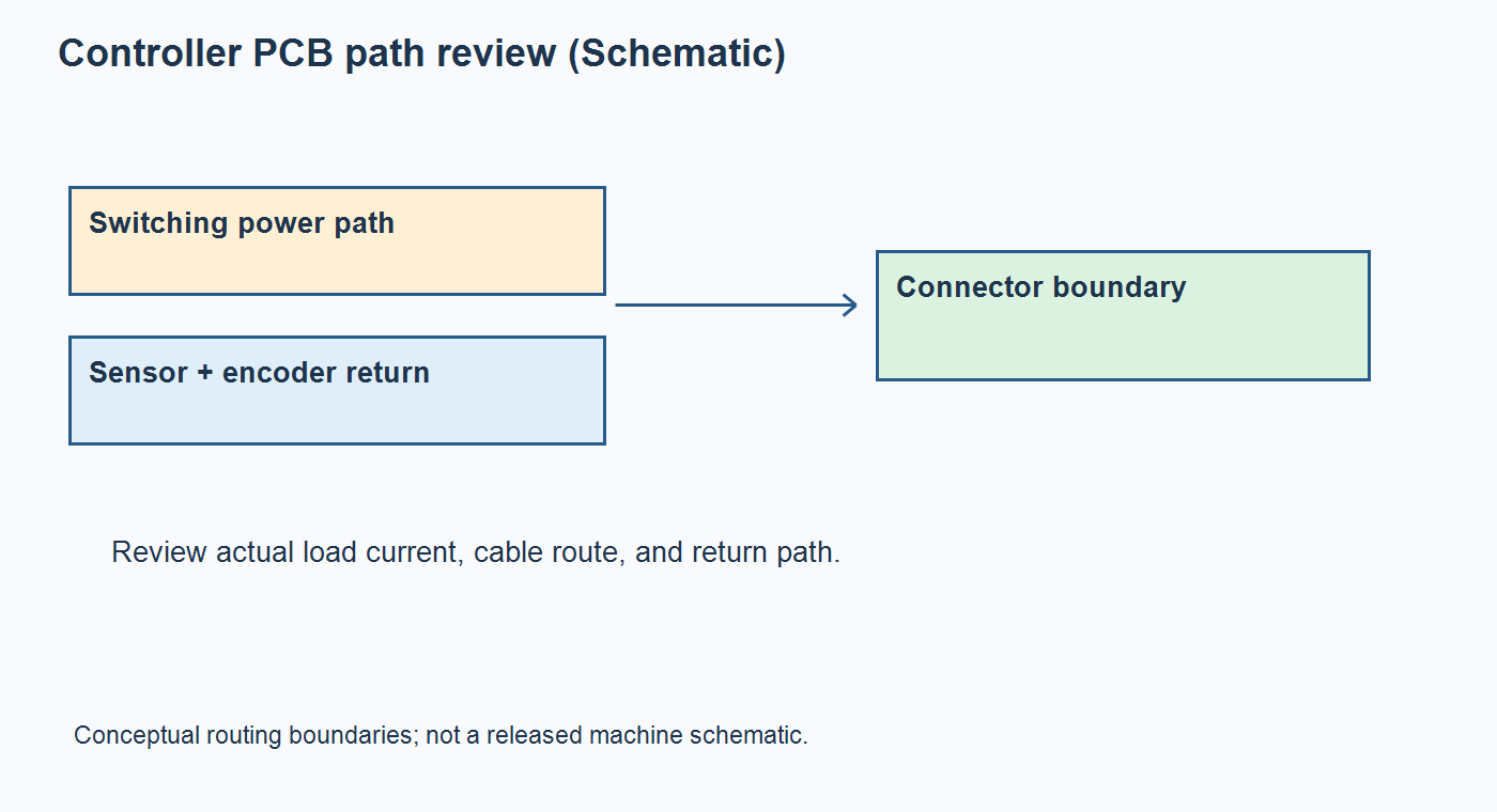
These four checks define the electrical intent before the fabrication drawing is optimized. If the machine cycle or harness is still changing, share the controller layout and load profile with the schematic and connector map so board and assembly assumptions can be reviewed before final routing.
Checks 5–8: reduce fabrication exceptions without weakening the design
5. Size copper from the real current and heat path. Define continuous and peak current, ambient, copper weight, acceptable temperature rise, and heat removal before selecting trace width or copper pour. Do not use a universal “motor trace width.” Where a terminal or switching device adds localized heat, review thermal vias and copper balance with the fabricator and assembler.
6. Use the fabricator’s standard drill and annular-ring window where possible. List finished-hole sizes, plating expectations and land dimensions. A hole or via that requires a special drill or leaves little registration margin can add process risk. The annular-ring DFM guide explains why the finished hole and drill allowance must be assessed together. IPC’s DFM profiles likewise separate producibility levels rather than presenting one universal minimum.
7. Check spacing against voltage, environment and process. Review conductor-to-conductor, pad-to-pad and board-edge distances for the actual working and transient voltages and contamination environment. The clearance required for a mains-connected heater interface is a different question from low-voltage sensor routing. Keep electrical safety requirements and fabricator line/space capability as separate checks; do not trade one away to fit a lower-cost process.
8. Keep mounting holes and board outlines manufacturable. Align hole positions with the released enclosure and service access. Reserve copper, component, and tooling clearance at edges and mounting hardware. Oddly shaped outlines, fragile tabs, and ambiguous slot callouts can affect routing, depaneling and assembly fixtures. If board shape is still changing, release the mechanical drawing with the same revision as the Gerbers.
Run a marked-up DFM report against these four items and close each deviation before release. The DFM report interpretation guide shows how to separate a build-blocking exception from a cost or yield improvement. A cost-saving change is useful only when the revised files and acceptance limits are under control.
Checks 9–12: avoid hidden assembly and test labor
9. Validate land patterns against the chosen components. Check package dimensions, pad geometry, solder-mask openings, stencil apertures and courtyard clearance with the actual BOM. IPC-7351B addresses land patterns, assembly and test access as linked design topics. A visually tidy footprint can still need hand rework if it ignores the supplier’s package drawing or inspection access.
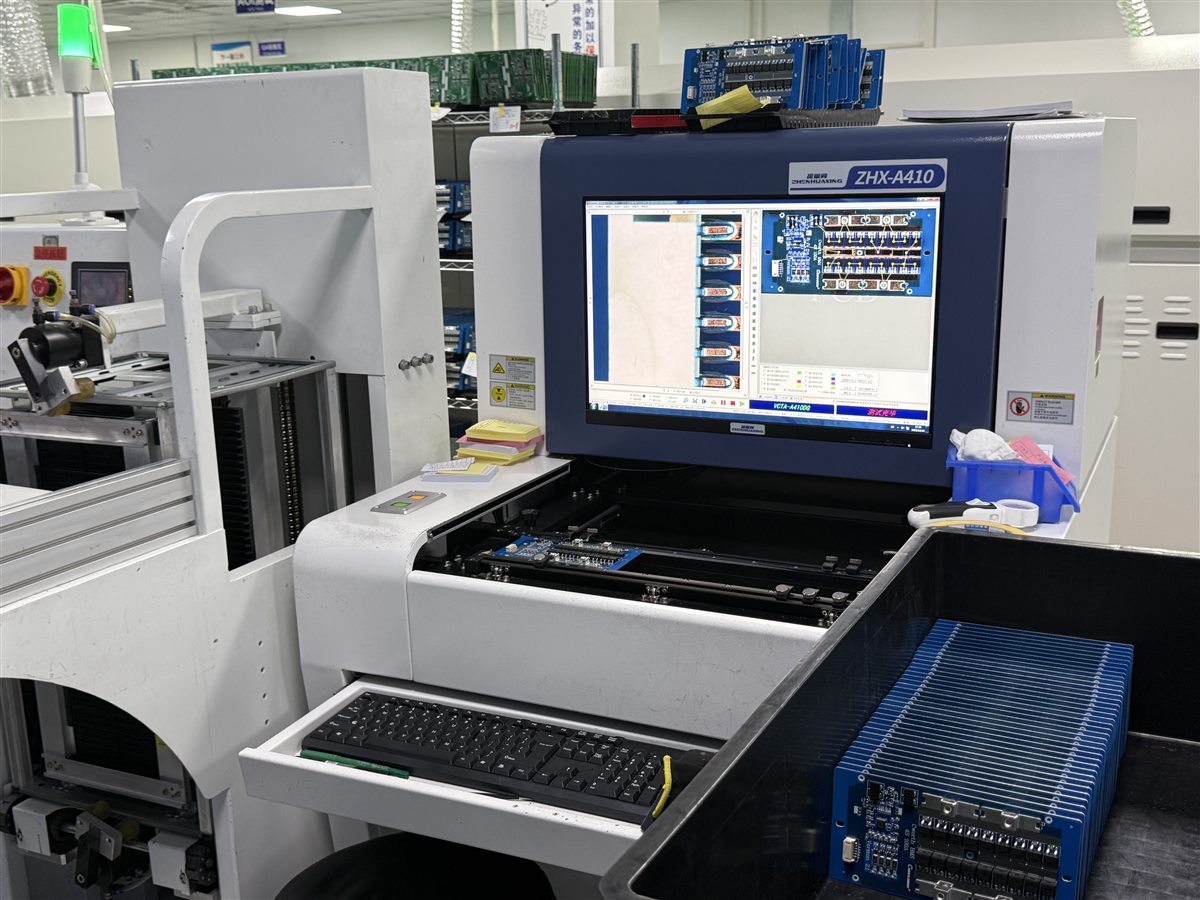
10. Preserve placement and inspection access. Place fiducials and polarized components so machine vision and assembly instructions can verify orientation. Keep tall terminals and cable hardware from blocking paste printing, placement, AOI views or rework tools. For a two-sided build, confirm component retention and sequence rather than assuming that every package can follow the same second-side reflow plan.
11. Design test points around the real production sequence. Decide what is measured on a bare board, after assembly and during machine-level functional test. Provide probe access to rails, sensor inputs, communications and critical output states, with fixture keepouts and a serial or lot record. The test-point release guide helps turn a schematic net into a reliable probe target. A finished board that is difficult to contact can consume more labor than a modest routing change saves.
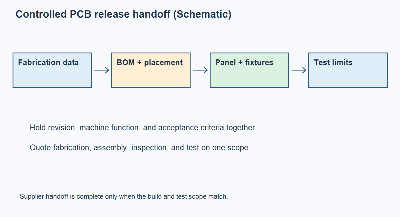
12. Release a usable panel and complete data package. Agree on board orientation, rails or tabs, fiducials, depaneling method, and fixture supports with the assembler. Supply fabrication files, drill data, stackup, controlled BOM and alternates, centroid/placement file, assembly drawings, firmware and a functional test description. A panel should reduce handling without placing connectors or fragile components at a break edge. See the panelization cost guide for the fabrication-to-assembly tradeoff.
Compare cost using the same released machine requirement
Use the 12 checks to create two controlled options where a change is genuinely optional: for example, a standard drill instead of a specialized via, or a revised connector location that simplifies the harness. Quote each option with the same volume, board class, component sourcing, assembly process, inspection, electrical test, fixture, and delivery scope. A fabricator’s lower board price is not a product saving if it raises harness work, rework, or functional-test time.
Ask the supplier to identify which proposed change affects board yield, part availability, setup, placement, manual insertion, AOI coverage, depaneling, or test cycle. Keep safety, EMC and function acceptance unchanged unless the OEM approves a design change. For a complete build, the full turnkey PCB assembly scope is a commercial starting point; confirm the actual fabrication, sourcing, assembly and test responsibilities in the RFQ.
When the design is released, send the released build package for a combined review: revision-controlled Gerbers, BOM, placement file, panel drawing, quantities, and test limits. The quotation should make open DFM issues and test ownership visible beside the price.
Conclusion: remove exceptions, then measure the whole build
Cost-saving DFM for a high-speed strapping controller is a controlled tradeoff, not a list of universally smaller dimensions. Map the machine boundary, protect feedback from switching paths, use qualified fabrication margins, and design for assembly and test. Compare the resulting board and PCBA options against the same functional and quality requirements before selecting the production revision.
Technical sources
- IPC DFM profiles — standards-based producibility levels and multiple design domains.
- IPC-7351B table of contents — land-pattern, assembly and test-access topics.
- Texas Instruments PCB layout guidance — switching-loop, return-path, EMI and thermal considerations.
- Analog Devices AN-1397 — exposed encoder-cable and motor-control interface EMC context.
Latest Blog
Contact Info
Phone: +86-755-82882936
Email: [email protected]
WhatsApp: +86-13570802455
Wechat: +86-13570802455
Address: 2nd floor,D Bldg.,Electric Link Technology Bldg.,Gongming,Guangming New Dist.,518106 Shenzhen, China