
Blister Packer Controller PCB: From I/O Map to Fabrication Release
Table of Conent
Table of Conent
A blister packer controller PCB is ready for fabrication only when its machine interfaces, electrical limits, connector map, and release files describe the same approved revision. Begin with the machine I/O list and assign each function to the PCB, an external PLC or drive, or a separate safety system. Then design the board for the actual signal levels and installation environment, review layout and test access, and inspect the exported fabrication and assembly package. A generic “servo controller” schematic cannot establish these boundaries for every blister machine.
This guide is for OEM electrical engineers and purchasing teams planning a new board or a redesign. It is a board-level handoff method, not a claim that a PCBA test proves package registration, seal integrity, or machine safety. Those outcomes need system-level acceptance criteria from the machine owner.
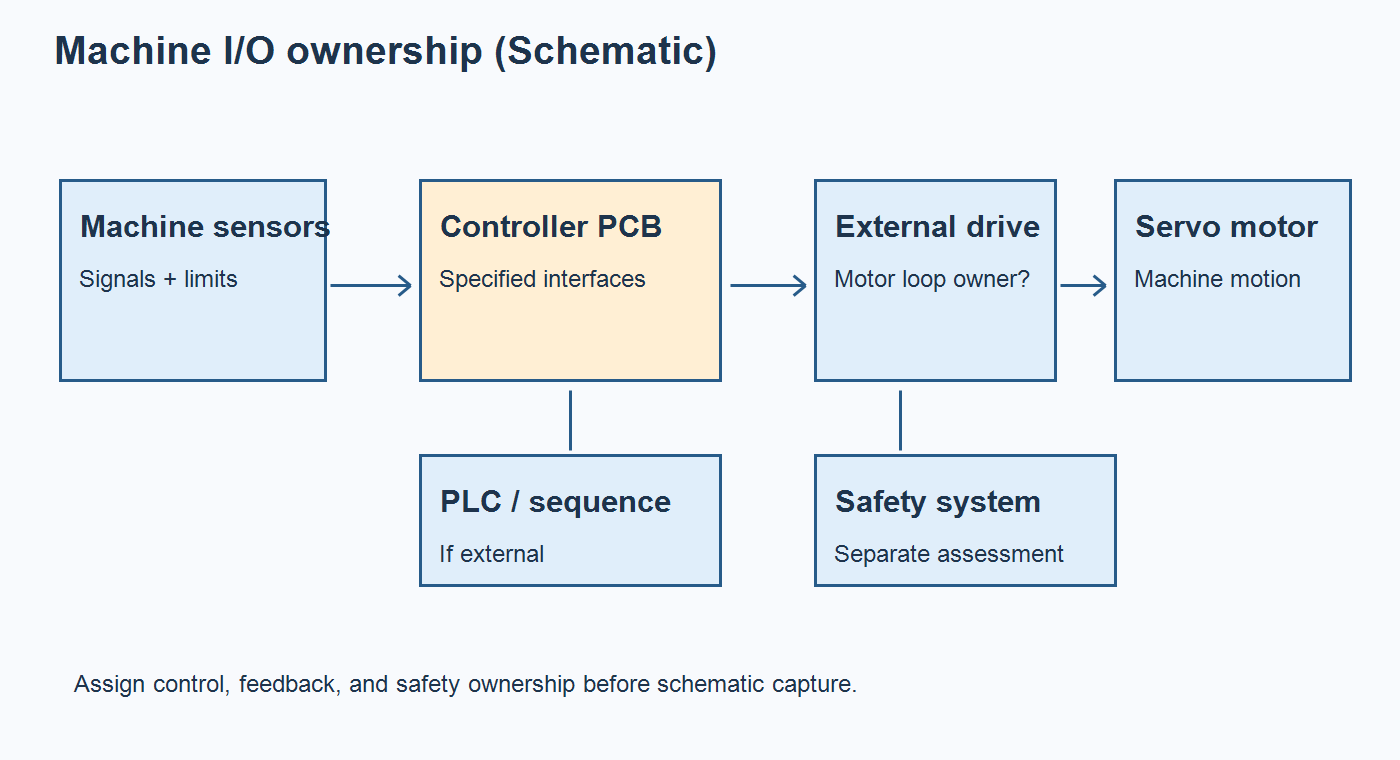
Define the PCB boundary before drawing blocks
The first drawing should show ownership, not just components. A blister line may include indexed motion, heater control, sensors, operator controls, and downstream equipment, but the location of those functions varies by architecture. An external servo drive may close the motor loop while the PCB provides isolated commands and status. A PLC may own sequence logic. Safety functions require an independently specified architecture; do not infer them from a general-purpose controller board.
For each interface, record the mating device, connector and pin, normal and fault voltages, current, timing or bandwidth, reference potential, cable length and shield termination, and what happens on loss of power or communication. The OEM should also state whether field wiring can be disconnected under power and what service technician access is required. These facts decide the circuit and layout; a net named “sensor input” does not.
A useful cross-check is the case packer controller functional-test scope. It concerns a different machine, but its separation between PCBA interfaces and machine acceptance is a sound way to frame a supplier discussion. Keep the blister machine’s actual pin map and acceptance conditions in its own controlled documents.
Turn the I/O list into a design and release decision table
An interface matrix makes omissions visible before layout. The examples below are conditional: they tell the team what evidence to request, not which circuits every blister packer must contain.
| Interface or boundary | OEM input needed before layout | PCB design or supplier evidence | Hold the release when |
|---|---|---|---|
| Servo command and feedback | Drive model, command type, encoder ownership, cable route, grounding scheme | Pin map, interface levels, EMC plan, and functional-test stimulus | It is unclear whether the PCB or external drive closes the loop |
| Field sensors and interlocks | Sensor type, supply, fault state, cable length, and required diagnostic behavior | Input protection and isolation decision, connector drawing, fault test | “Input” lacks voltage, reference, or fault limits |
| Heater or actuator control | Whether power switching is on the board or in external hardware; load and thermal limits | Power-stage layout review if applicable, thermal plan, and load-test boundary | PCB copper or connector rating is assumed without a specified load |
| Safety boundary | Machine risk assessment and the designated safety controller or circuit | Explicit interface and exclusion statement in the PCB specification | A standard I/O test is being treated as safety validation |
| Service and production test | Accessible connectors, firmware state, fixture access, pass/fail limits | Test-point map, fixture protocol, and revision-matched test record | The assembler must guess how to power or exercise the board |
The table links a design decision to an approvable record. For example, a low-voltage pulse/direction command to a purchased servo drive is a different board problem from an integrated power inverter. Neither should be specified from the phrase “servo-driven” alone. Texas Instruments discusses industrial encoder-interface EMC considerations; apply that guidance only when the board actually contains that receiver and the chosen device and cable conditions match.
If the architecture is still being set, send the I/O ownership matrix, candidate connectors, machine wiring limits, and open EMC questions for a board manufacturability review. The team can identify which assumptions affect layer stack, assembly, test fixture, and pricing before a build package is frozen.
Route power, returns, and field connections for the chosen architecture
Layout follows the actual circuit partition. Keep noisy switching current loops compact if the PCB carries switching power; if an external drive carries those currents, focus the controller-board review on command, feedback, field supply, and cable entry instead. Do not apply a motor-driver placement rule to a board that does not contain a motor driver. Texas Instruments’ motor-driver layout guidance is pertinent only when such a power stage is part of the design.
Identify where each field signal returns, where protection acts, and how chassis and signal references are intended to meet. Cable shields and transient protection are system choices that should be checked against the selected components and installation environment. Analog Devices’ industrial input protection example illustrates that input protection and isolation depend on the interface specification. It does not supply a universal schematic for this machine.
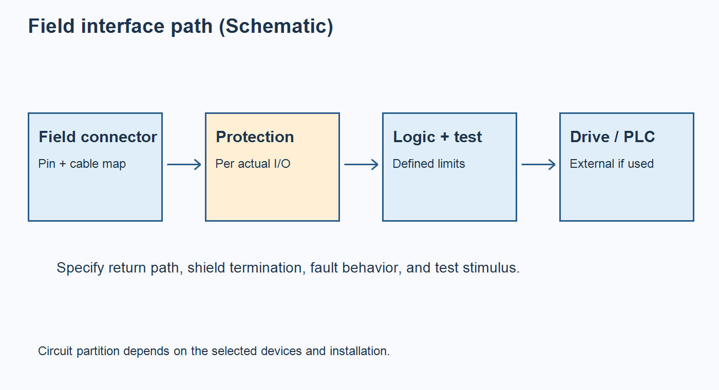
Reserve room for connector mating, strain relief, isolation distances appropriate to the specified circuit, mounting hardware, and probing after assembly. Mark which pins remain available when the board is inside its enclosure. Confirm any high-current path with current, copper, thermal, and connector calculations tied to the selected stackup. A broad “industrial PCB” label cannot replace those values. For a board whose mechanical fit or conductor capacity is sensitive to thickness, use the PCB thickness selection guide alongside the actual enclosure and fabrication notes.
Release files that preserve the I/O intent
A Gerber archive is necessary for many fabrication workflows, but it does not carry all assembly and machine-interface intent. IPC’s PCBA documentation checklist identifies the need for a coherent set of design and assembly data. Provide the approved schematic, connector pin map, fabrication notes, layer stack, copper and drill outputs, BOM with approved substitutions, placement data, assembly drawing, firmware/test requirements, and an exception log as applicable. Resolve conflicting revisions before an RFQ or build release.
Open the exported fabrication files in an independent CAM viewer. Check outline, plated and nonplated holes, layer order, solder mask and paste, polarity marks, and tooling or panel instructions against the latest board drawing. The Gerber, ODB++, and IPC-2581 comparison explains why the file format is only one part of the handoff. The PCB assembly drawing checklist can help align reference designators, polarity, special processes, and inspection notes with the BOM and placement file.
The official OrinewPCB video below covers five inputs for a more accurate PCB quote, including a complete Gerber package and drilling data. It is a general fabrication and quotation guide, not a blister-machine design demonstration.
Plan board tests without claiming machine validation
A functional test should exercise specified board inputs and outputs at defined supply and load conditions. Match fixture connector pins to the released pin map. Record firmware and board revision, stimulus, expected response, tolerances, failure indication, and whether calibration belongs to the PCB or the machine. Where an external PLC or drive owns behavior, test the communication or command boundary at the PCBA, then leave coordinated motion and package quality to machine commissioning.
Ask the assembler which tests are feasible on an uninstalled board and which require a representative harness or load. A successful power-on check alone cannot establish the board’s fault response; conversely, a board-level fault response does not certify the whole packaging machine. Clarifying this division early reduces ambiguous acceptance language in the purchase order. Full turnkey PCB assembly scope is relevant when one supplier is expected to procure parts, build the PCBA, and coordinate the agreed board-level test.
Before release, close the I/O ownership matrix, approve the connector and firmware revisions, inspect the exported files, and agree on board-level test evidence. For a complete assembly evaluation, provide the revision-matched schematic, fabrication archive, BOM, placement data, pin map, and test limits for an assembly and quotation review. The ensuing review can confirm build assumptions, test responsibilities, and any missing data before production scheduling.
Latest Blog
Contact Info
Phone: +86-755-82882936
Email: [email protected]
WhatsApp: +86-13570802455
Wechat: +86-13570802455
Address: 2nd floor,D Bldg.,Electric Link Technology Bldg.,Gongming,Guangming New Dist.,518106 Shenzhen, China