
Bag Sealer Controller PCB Stackup: Choose Layers and Copper
Table of Conent
Table of Conent
Choose a bag sealer controller PCB stackup from the loads and return paths that are actually on the board, not from the word “servo” in the machine description. First establish whether the servo drive and heater power switching are on this PCB or in external modules. If the board only sends commands and reads sensors, its layer count may be driven by routing density, stable signal reference, isolation, and connector access. If it carries motor or heater current, the team must also size finished copper conductors for peak and continuous current, voltage drop, allowable temperature rise, and the complete path through vias and connectors. No fixed layer count or copper weight fits all architectures.
The useful purchasing output is a revision-controlled stackup and load schedule that a fabricator and assembler can check. The machine owner remains responsible for sealing quality and system safety; a PCB temperature or continuity test does not establish either.
Separate the control board from the motor and heater power path
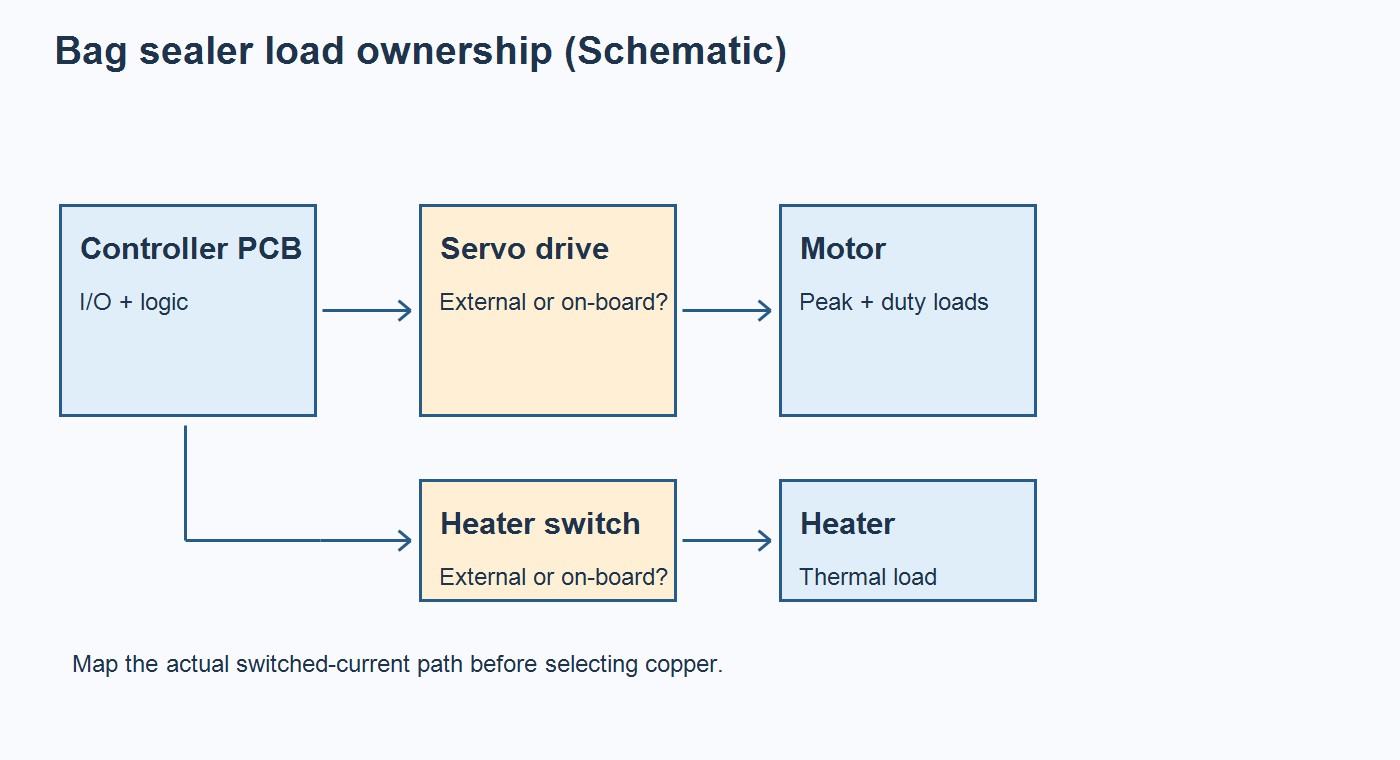
Start by assigning each load to the actual hardware that switches it. An external servo drive may carry the motor phase current while the controller PCB carries only logic-level commands, status, and field I/O. A heater may be switched by a separate power module or by devices mounted on the board. Those alternatives lead to different copper, thermal, protection, and isolation requirements. Specify the drive model, heater supply and switching element, cable lengths, enclosure, and grounding arrangement before selecting a stackup.
Draw the complete high-current loop from source through switch, load, return, connector, and protection device. Include start-up, stall, fault, and regenerative cases where they apply; do not treat the steady operating current as the only design input. If the motor power stays outside the PCB, avoid charging the controller design for heavy copper that its traces never need. If any power stage is on the PCB, follow the selected component maker’s layout and thermal guidance. Texas Instruments’ motor-driver layout guide explains the role of compact switching loops, local capacitors, ground paths, and thermal copper for such a stage.
The controller power-path and copper-weight guide provides a related current-path checklist for a different machine. Use its method of checking path bottlenecks, but substitute the bag sealer’s measured or specified load profile rather than copying another product’s values.
Select layer count for reference paths and routing space
Layer count is a signal-integrity and manufacturability decision as well as a routing-capacity decision. A two-layer board may be reasonable when power conversion is external, signal count is modest, and the layout can preserve sufficiently short, controlled return paths. Adding layers can provide a more continuous reference plane and cleaner separation between power and sensing or communication circuits, but the chosen layer count must follow the actual placement and net classes. More layers alone do not repair a return path interrupted by a split or an awkward connector location.
For a mixed-signal controller, place sensitive sensor and reference circuitry away from switching nodes and plan how each signal returns. Analog Devices’ mixed-signal PCB layout guidance explains why a continuous, low-impedance reference and block placement matter; it also cautions against treating split analog and digital grounds as an automatic cure. Choose grounding around the selected devices and current paths, then check it in the routed design.
Compare a candidate two-layer implementation with a four-layer concept on paper: connector escape, return continuity, heat flow, test access, and board outline. An added plane can be valuable if these are hard to maintain on two layers. A six-layer stack can be justified by dense routing or multiple protected interfaces, but should not be selected solely because the machine has a servo. The existing two-layer board guide and six-layer stackup guide cover the broader fabrication trade-offs; this article applies the choice to the bag sealer’s load boundaries.
Size finished copper for the whole current path
Copper weight on a purchase drawing should describe the finished conductor, not an unqualified starting foil. The design owner must set current, permitted voltage drop, and temperature-rise targets and have the fabricator confirm finished copper and trace geometry. IPC-2152 is a current-carrying-capacity guide relating current, conductor size, and acceptable temperature rise. Its published scope supports using those variables together; it does not make a single trace-width rule universal.
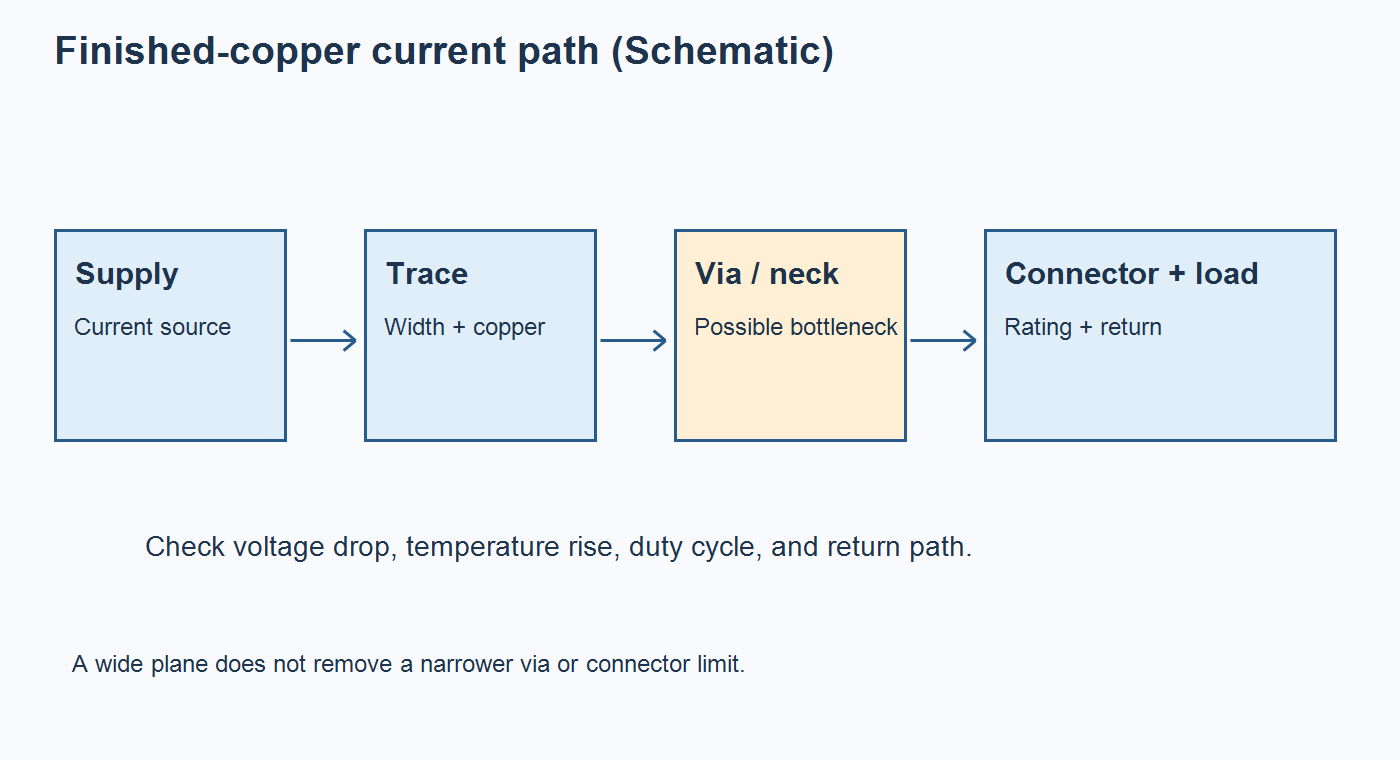
Review the narrowest point of the circuit, including pad neck-downs, thermal reliefs, vias, fuse holders, terminal pins, and connector ratings. A wide plane connected through one undersized via remains constrained at the via. Consider whether the conductor is external or internal, the surrounding copper, ambient and enclosure conditions, duty cycle, and adjacent heat sources. The allowable temperature rise is a product decision, not a value to infer from an online width calculator.
Separate electrical current capacity from heat removal at an active device. A copper path may carry the specified current while the switch package exceeds its allowed junction temperature in the closed enclosure. Conversely, a larger thermal pour may improve device cooling without fixing a connector that limits current. Put both the path calculation and a worst-case board-temperature measurement in the first-article plan; record where the probes sit and what operating state the test represents.
When a candidate board carries a heater or motor load, share the load schedule, connector ratings, proposed stackup, and allowable temperature rise for a fabrication review. That review can identify whether width, added copper, a different connector, a separate power board, or a revised enclosure assumption is the practical next change before the assembly quote is fixed.
Use a decision matrix before locking the purchase stackup
The following matrix turns the architecture and thermal questions into an RFQ hold point. It is conditional guidance: the entries do not prescribe a stackup or certify a specific sealer design.
| Observed design condition | Layer and copper implication | Evidence to request | Release hold |
|---|---|---|---|
| External drive and heater module; controller handles low-power I/O | Start with routing and return-path review; extra copper may have little value | Interface pin map, drive/module specifications, placement and return-path review | Power ownership or field wiring limits are unknown |
| On-board motor or heater switching | Evaluate power-loop geometry, copper temperature rise, thermal exit, and connector limits | Load profile, selected device data, finished-copper stackup, thermal calculation and test plan | Only nominal current or starting foil is specified |
| Low-level sensor signals near switching loads | Prioritize continuous reference, separation and measured noise margin; more layers may help | Net classes, return map, sensor limits, layout review and functional test | A signal crosses a plane gap or return path is undefined |
| Many field connectors in a compact enclosure | Check routing escape and mechanical access before adding layers | Connector drawings, enclosure model, harness bend and test-fixture access | A feasible routing pattern depends on inaccessible connectors |
| Proposed thick copper | Confirm fine-feature and soldering implications with the fabricator and assembler | Approved stackup, minimum features, thermal relief and assembly review | Supplier has not accepted finished-copper and feature requirements |
A heavier conductor can reduce resistance but can also affect etching allowances, fine-pitch features, thermal balance, and assembly heating. The thick-copper PCB service scope is relevant only when current-path calculations and supplier capability justify that process. It is not a default substitute for routing discipline.
Procurement should ask for the fabricator’s proposed layer construction and finished-copper tolerance before approving the board price. If a supplier changes dielectric thickness, copper thickness, or via construction to meet its process window, the electrical owner should review the changed return path, conductor loss, and mechanical thickness. The assembly owner should review the same revision for solderability and component fit. This keeps a cheaper fabrication alternative from silently changing the test baseline.
Release one stackup revision with assembly and test evidence
Freeze the actual layer order, finished board thickness, copper specification by layer, board outline, drill and via requirements, and controlled interface drawings as one revision. Send fabrication files with the BOM, placement data, assembly drawing, connector list, and board-level test instructions. Ask the fabricator to flag any proposed material or copper substitution before fabrication. A layer change that alters routing or via structure reopens both electrical and assembly review.
Test the board at defined supply and load conditions, including the operating states that exercise the specified motor or heater interface. Record board revision, firmware, fixture, temperature measurement locations, and pass/fail limits. Where the drive and heater power are external, verify the command and status boundary on the board; machine seal quality, motion timing, and safety remain system-level acceptance tasks. The site’s full turnkey PCB assembly scope can support a coordinated fabrication, sourcing, assembly, and agreed board-test discussion.
The practical conclusion is to define power ownership first, then select layer count for real return paths and copper for verified current and thermal limits. For a complete build evaluation, provide the approved stackup, fabrication files, BOM, placement data, load cases, and board-test limits for assembly and quotation review. The resulting discussion can confirm fabrication constraints and test responsibilities before the release is scheduled.
Latest Blog
Contact Info
Phone: +86-755-82882936
Email: [email protected]
WhatsApp: +86-13570802455
Wechat: +86-13570802455
Address: 2nd floor,D Bldg.,Electric Link Technology Bldg.,Gongming,Guangming New Dist.,518106 Shenzhen, China