
Embedded Passives in PCBs: Decide Which Resistors and Capacitors Belong Inside
Table of Conent
Table of Conent
Embed a resistor or capacitor in a PCB only when the electrical benefit and released manufacturing controls justify moving that part into the laminate. Buried resistors can save surface area or shorten a sensitive connection, while a distributed embedded capacitance layer can support power-distribution behavior. Neither is a drop-in replacement for every discrete resistor or MLCC. The choice changes fabrication, tolerance control, inspection, repair, and the way purchasing compares quotes.
For an OEM review, start with the exact circuit function and acceptable variation. Then ask the fabricator to show a feasible stackup, material system, panel test strategy, and yield assumptions. Keep the assembler’s placement and test savings on the same cost sheet as the fabricator’s added processing and scrap exposure.
Separate embedded resistors from embedded capacitance
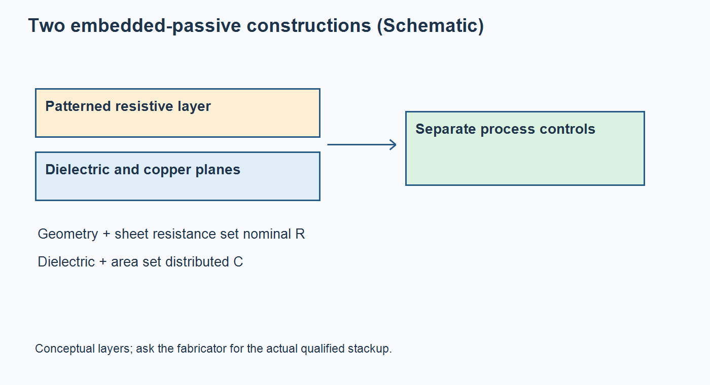
An embedded resistor uses a resistive material patterned within the board construction. Its nominal value depends on the material’s sheet resistance and the geometry of the finished element. A broad embedded capacitance layer, by contrast, places a thin dielectric between conductive planes and is often considered as part of a power distribution network. A small, individually defined buried capacitor is a different design and process proposition. Specify which construction the drawing calls for before a supplier prices “embedded passives.”
The reason for embedding must be measurable. Is the goal a shorter high-frequency path, local power-plane capacitance, removal of an otherwise crowded surface component, or a lower assembled-unit cost at volume? A layout sketch alone cannot establish any of these benefits. Compare an embedded candidate with the discrete baseline using the same circuit requirements, board outline, production volume, test plan, and field-service expectations.
Turn the circuit requirement into a fabrication decision
Use the table as a first RFQ filter. The listed controls are questions for a qualified fabricator, not promises that one material system can meet every value, geometry, voltage, or reliability target. If an item’s tolerance, voltage stress, or replacement need is critical, retain the discrete reference design until measured prototype data supports the embedded version.
| Candidate function | Potential value | Evidence to request before release | Decision if evidence is weak |
|---|---|---|---|
| Fixed bias or termination resistor | Surface space and connection length may improve. | Material grade, sheet resistance, finished geometry, resistance distribution, trim plan if used, temperature behavior, and accessible test method. | Keep a discrete resistor or reserve an alternate footprint. |
| Precision or service-adjustable resistor | Embedding may still help a constrained layout. | Worst-case circuit tolerance, drift, calibration sequence, rework path, and lot acceptance limits. | Prefer a discrete or adjustable part when value correction is needed after fabrication. |
| Distributed plane capacitance | Can add closely coupled capacitance across a power/return plane pair. | Dielectric thickness and material data, plane area, voltage rating, impedance target, via/plane geometry, and validation across frequency. | Retain discrete decoupling network until PDN measurement supports change. |
| Local discrete-equivalent capacitor | May free surface area in a specialized construction. | Achievable value and tolerance, leakage, breakdown, environmental behavior, inspection, and replacement strategy. | Keep the MLCC or other discrete part when the embedded process is unqualified. |
For a comparison that procurement can audit, keep the discrete and embedded designs as separate revisions or quote options. Record the quantity of removed placements, altered layer count, added material, test coupons, expected fabrication yield, assembly steps, and failure-analysis cost. The cheapest bare-board quotation can produce a more expensive qualified assembly, and fewer placed parts do not guarantee a lower total cost. The PCB quote comparison guide provides a framework for comparing delivered rather than headline cost.
Specify resistor geometry and tolerance without assuming a nominal value is enough
For a simple rectangular resistive element, a useful first-order relation is resistance equals sheet resistance multiplied by length divided by width. Quantic Ohmega describes this relationship for its resistive materials. The equation is a starting point, not a released tolerance model: material variation, etch definition, contact geometry, trim, temperature coefficient, and subsequent thermal processing can affect finished resistance. Ask the material supplier and fabricator for the applicable material grade and process capability at the proposed shape and value.
Identify whether values are measured on production boards, coupons, or both; whether laser or other trimming is in scope; and who owns the acceptance limit. A circuit that uses several embedded resistors as a matched ratio may need a different acceptance method from one that only limits each absolute value. Place measurement access in the design while the layer stack can still be changed. The PCB test-point design guide is relevant to accessible net selection, but buried element acceptance may also require dedicated coupons or intermediate-process tests agreed with the fabricator.
If the value is corrected during system calibration, put the calibration step and its allowed range in the assembly test specification. Otherwise purchasing may remove a discrete resistor from the BOM and miss the added test time or the need to reject uncorrectable boards.
Validate embedded capacitance as a power-network change
Capacitance depends on dielectric properties, thickness, and effective plane area. A broad plane pair can behave differently from a nearby discrete MLCC once mounting inductance, via geometry, frequency, and the rest of the power distribution network are included. Do not delete the discrete decoupling set from a schematic simply because a thin dielectric layer is present. Simulate or measure the rail impedance and transient response against the device’s actual target, with the fabricated stackup represented.
Request the exact material data sheet, approved layer locations, voltage and isolation requirements, and the method used to verify finished-board capacitance or impedance. A data sheet for a flexible circuit film is not automatically evidence for a rigid-board stackup. Lock the material and dielectric thickness on the released drawing, and ask what substitutions require requalification. For discrete capacitors still in the design, the MLCC bias and alternate review explains why nominal capacitance alone is insufficient for an approved substitution.
Before a prototype run, send the proposed stackup, resistor values, rail impedance target, annual volume, and test access plan for a fabrication and assembly feasibility review. This first review should resolve material availability and the measurements required to compare the embedded and discrete options.
Release test access and acceptance limits with the artwork
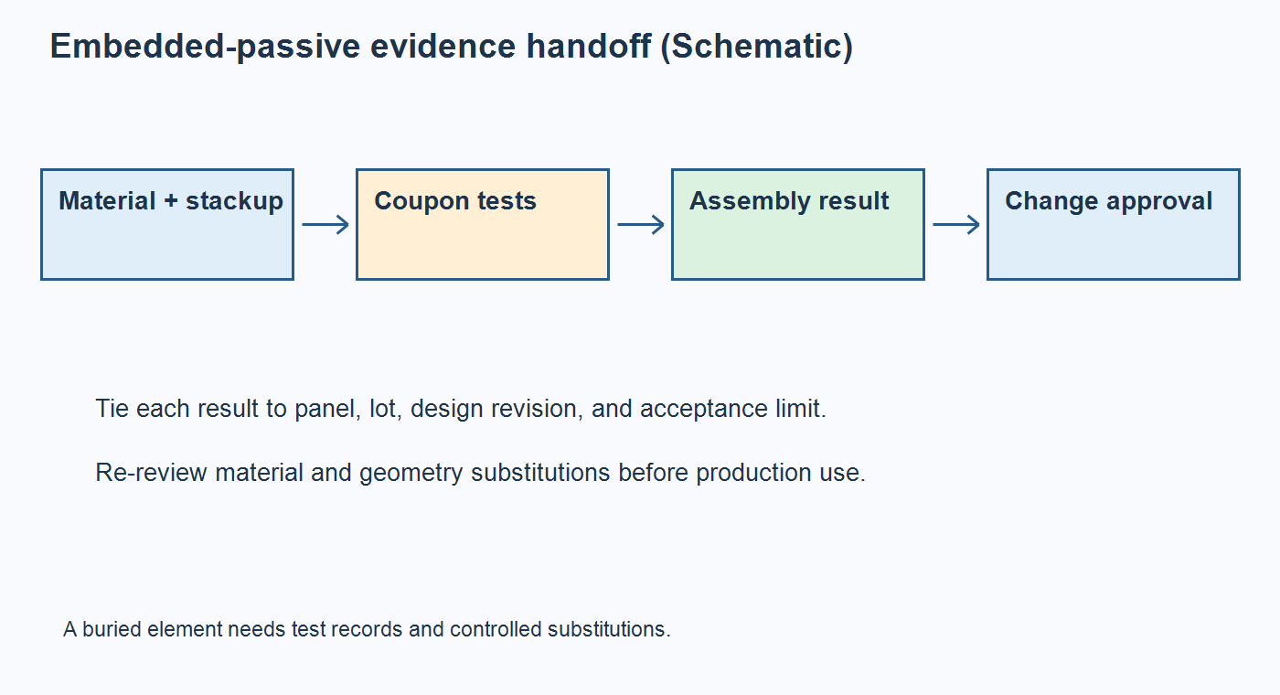
Once the passive is buried, ordinary visual inspection cannot tell whether its electrical value is acceptable. Define what can be measured before lamination, on finished bare boards, and after assembly. Keep a traceable link between coupon results, panel, board serial or lot, material batch, and the released design revision. A failed functional test after assembly should be diagnosable without guessing whether the embedded element, an assembled component, or a solder connection caused the fault.
For resistors, list value windows at a named stage and temperature, sampling or 100% test requirement, test fixture, and disposition for out-of-limit elements. For capacitance layers, list the applicable isolation, voltage, capacitance or impedance checks and their measurement conditions. Confirm that test pads, temporary tabs, or coupons do not compromise the intended signal path or panel yield. IPC-6012F explicitly includes embedded passive circuitry in the rigid-board qualification and performance context; the purchase drawing must still state the product-specific class, construction, acceptance criteria, and agreed tests.
Price board yield and assembly savings together
Embedding can move cost from the assembly line into board fabrication. The board may require a specialized material, additional registration or lamination controls, intermediate electrical checks, or a different panel utilization. At the same time, fewer placed components can reduce purchase, handling, placement, and solder-joint exposure. The balance depends on volume and process yield; there is no universal crossover quantity.
Ask for two comparable quote columns: a discrete baseline and an embedded variant. Each should show board fabrication, material procurement, assembly placements, electrical test, expected yield basis, tooling or qualification, scrap responsibility, and lead-time exposure. A supplier’s yield assumption deserves its own line because a buried defect may scrap an otherwise completed multilayer board. The IPC technical paper on embedded passives and total product cost supports evaluating fabrication and assembly together rather than treating placement savings alone as the answer.
If one supplier fabricates and another assembles, agree which party owns failed-board analysis and which test record travels with each lot. The PCB lamination overview helps frame why a layer construction change belongs in the fabrication handoff. A full turnkey PCB assembly quotation can consolidate material, fabrication, sourcing, assembly, and agreed test scope; confirm the actual embedded-passive capability and division of responsibility for this specific design.
Build a controlled release package before changing the BOM
The OEM’s package should include the discrete reference design, circuit performance target, stackup and material specification, layer artwork, resistor geometry and value schedule, capacitor plane definition, test access and coupons, acceptance limits, lot traceability, and agreed substitution rules. Mark embedded passives clearly in the BOM and drawing so an assembler does not order a missing discrete item or treat an intentionally vacant footprint as a placement defect.
Prototype review should compare measured electrical performance and actual yields from both options. Record any calibration step, reliability test, failure analysis, and approved alternates. Revisit evidence when the resistive film, capacitor dielectric, laminate, layer spacing, geometry, or fabrication site changes. A customer should approve those changes against the released requirements, because a material substitution can preserve an apparent nominal value while changing variation or long-term behavior.
Conclusion: require measured value before claiming saved space or cost
Embedded passives are useful when a defined electrical or layout benefit survives a real fabrication and assembly comparison. Release the material system, stackup, tolerances, test access, yield basis, and change-control rules with the circuit. Then decide whether the buried construction beats a discrete alternative on the performance and delivered cost that matter to the product.
For an RFQ, share both design options, target volumes, material constraints, acceptance windows, and the desired test ownership. A comparable response should state the proposed board construction, assembly savings, qualification work, and unresolved risks before the embedded variant becomes the production BOM.
Source notes
- IPC, IPC-6012F release — embedded passive circuitry within rigid-board performance scope.
- IPC-2316 design guide table of contents — embedded passive design topics and scope.
- Quantic Ohmega resistive material overview — sheet resistance and resistor geometry relationship.
- IPC technical paper, embedded passives and total product cost — manufacturing and assembly cost context.
Latest Blog

Contact Info
Phone: +86-755-82882936
Email: [email protected]
WhatsApp: +86-13570802455
Wechat: +86-13570802455
Address: 2nd floor,D Bldg.,Electric Link Technology Bldg.,Gongming,Guangming New Dist.,518106 Shenzhen, China