
PCB Busbar Interfaces: Specify Joints, Supports, and Tests
Table of Conent
Table of Conent
PCB busbar design succeeds when the joint, board transition, mechanical support, and acceptance test are specified together. A large copper bar does not establish the current rating of its connection to a printed circuit board. Select the terminal architecture first, release its required footprint and finished-hole conditions, then check the assembled hardware, tool access, and electrical loss under defined operating conditions. Treat the busbar-to-board interface as a controlled assembly, rather than another copper feature in the layout.
This guide is for OEM engineers and buyers moving a power-electronics PCBA into production. It covers externally attached conductors and terminals, not every embedded-busbar board technology. The practical question is which files and evidence must accompany the PCB so the assembler can reproduce the intended connection. Product-specific drawings and application instructions remain the authority for dimensions, processing limits, and qualification.
Choose the joint architecture before releasing the PCB
Choose the connection system before freezing holes and copper. A soldered tab, a specified press-fit terminal, a bolted power contact, and a separable connector require different interfaces. Changing between them after the bare board is ordered can change the fabrication data, tooling, inspection access, and assembly sequence.
For example, TE’s press-fit explanation describes compliant terminals that deform during insertion. That is a defined terminal-to-hole system, not permission to force an arbitrary rigid pin into a plated hole. Other suppliers offer different press-fit constructions; use the specification for the exact selected part.
| Architecture | What must be frozen | Assembly evidence to agree |
|---|---|---|
| Soldered tab or power terminal | Part number, land/hole geometry, solderable finish, joint access, and thermal process | Approved process setup and inspection criteria for the actual joint |
| Specified press-fit terminal | Terminal revision, finished-hole and plating requirements, board thickness, support and insertion tooling | Seating and process records required by the terminal supplier |
| Bolted interface through a rated power contact | Contact and bar drawings, fastener stack, surface conditions, support, and tightening instruction | Correct hardware and controlled assembly record, followed by specified electrical checks |
| Separable busbar connector | Mating pair, alignment, engagement, mounting method, and permissible system loads | Mating/retention checks and electrical evidence under the agreed configuration |
Keep substitutions tied to that architecture. A terminal with the same thread or nominal current may have a different footprint, seating condition, or processing instruction. Require a change review of the terminal, board interface, assembly setup, and evidence together. Procurement can then distinguish an approved alternate from a part that merely looks interchangeable on a purchasing list.
Separable designs are a real option: Amphenol’s PwrBlok family combines a spring contact interface with specified press-fit mounting options. Its product data does not establish the rating of a different connector or your completed PCB. Evaluate the whole selected configuration.
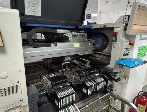
For soldered parts, plan when the power hardware enters the build and what remains accessible afterward. The SMT and through-hole assembly sequence illustrates why a late mechanical choice can affect process order. Do not assume a large terminal can use an unchanged process simply because it fits the board.
Budget the joint and transition separately
Allocate loss to each physical segment instead of assigning one resistance to the entire copper path. Identify the bar, contact interface, terminal, PCB land, neck-down, layer transition, and return path. This creates a useful investigation map when the assembly has an unexpected voltage drop or hot spot.
A hypothetical DC example makes the distinction clear. At an assumed 50 A, a 0.2 mΩ joint produces a 10 mV drop and 0.5 W of dissipation: V = IR and P = I²R. If that resistance becomes 1.0 mΩ at the same current, the figures become 50 mV and 2.5 W. These are arithmetic examples, not measured OrinewPCB results, acceptable joint limits, or a predicted temperature rise.
The comparison tells the designer where to reserve measurement access. A wider conductor cannot by itself repair an unsuitable interface. Conversely, a low-resistance contact cannot compensate for a narrow PCB transition. For changing or pulsed loads, record the waveform and thermal boundary instead of treating the example’s steady DC condition as universal.
Define the load path and assembly access in 3D
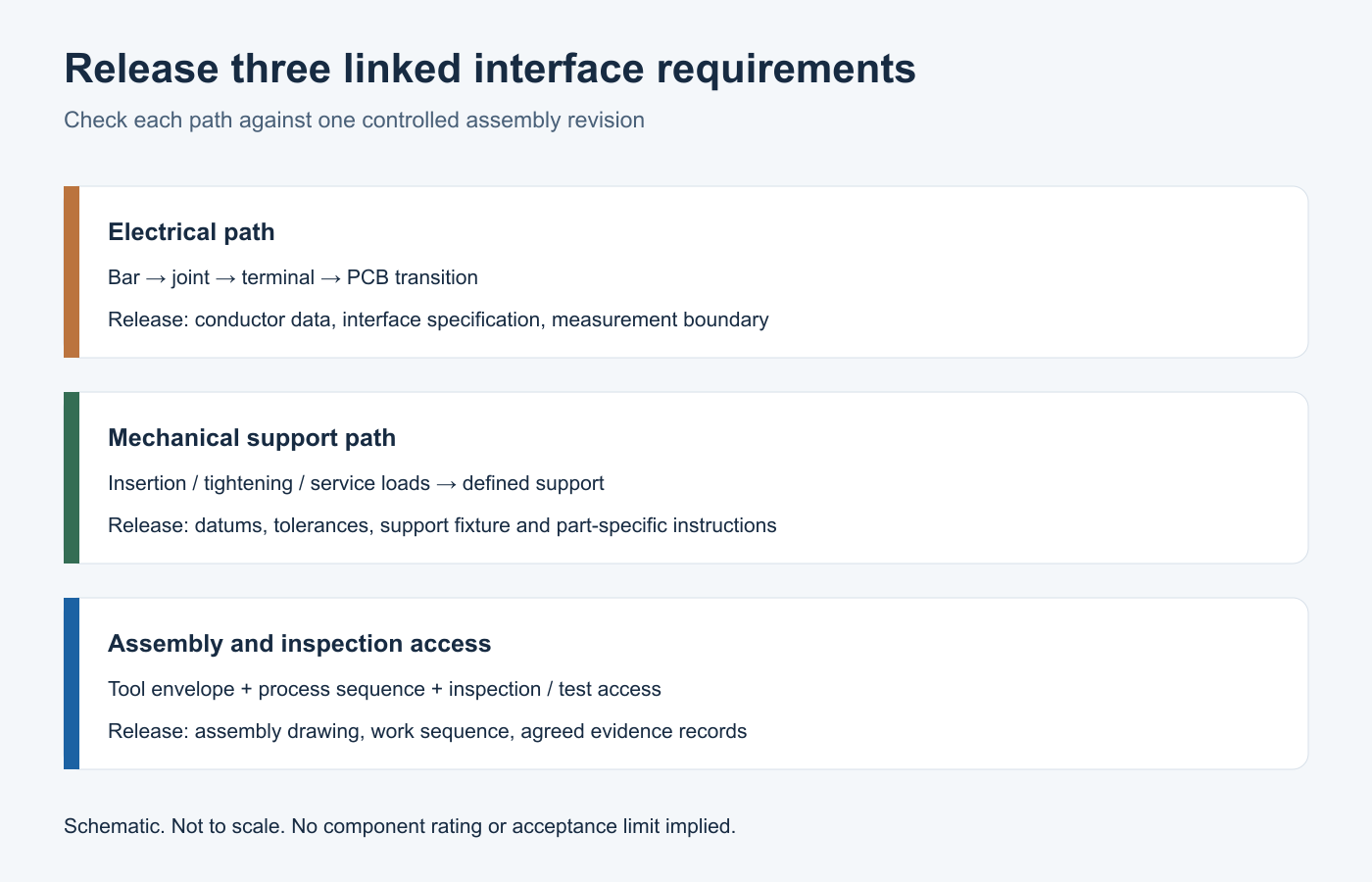
Specify how insertion, tightening, harness movement, and installed service loads reach the support structure. Do not leave the assembler to infer the intended mechanical restraint from the copper artwork. Review the PCB and mating conductor against the same datum system, including component and enclosure tolerances.
If the support or datum review exposes a design-to-build gap, share the interface drawing and component restrictions with the PCB data so the assembly approach can be reviewed and any separate tooling requirements identified.
Würth Elektronik ICS’s acceptance guidelines require observing the relevant hole specification, protecting the PCB against bending during press-fitting, applying the insertion force in the specified direction, and respecting the permitted torque. These are supplier-specific processing controls. They are not generic values for every power terminal.
Model the support nest, insertion punch, driver or wrench, and inspection line of sight. A connection can fit in the enclosure yet be impossible to assemble in the planned order. Check whether the bar blocks access to a nut, hides the solder joint, or prevents the fixture from supporting the insertion area. Agree the sequence before committing the panel layout.
Check insulation around the assembled hardware
Review spacing on the complete assembly, including the bar, fasteners, washers, terminals, and nearby conductive enclosure parts. A spacing rule applied only to PCB traces can miss the closest path after hardware is installed. Include permitted movement and dimensional tolerances in the mechanical review.
Clearance is the shortest path through air between relevant potentials; creepage follows an insulating surface. Phoenix Contact’s insulation-test explanation shows that the required distances depend on electrical and environmental classifications, not only a nominal voltage. Its terminal-block test tables apply to their stated context; do not transplant a value into an unrelated power assembly.
Record the applicable product requirements, working and transient voltages, insulation function, pollution assumptions, material information, and operating environment for design approval. The PCB creepage and clearance review provides a broader framework. A slot, coating, or connector pitch should not be treated as automatic approval of the assembled insulation system.
Measure the interface you intend to accept
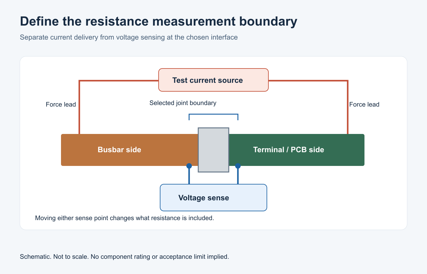
Define the sense points before setting a resistance limit. For low-resistance work, a two-wire reading includes lead resistance; a four-wire Kelvin arrangement uses separate current and voltage connections. Tektronix’s low-resistance guidance explains why sense placement, offsets, and measurement conditions matter.
Put the sense boundary on the drawing. Sensing across the complete bar-to-board path answers a different question from sensing immediately across one contact. Record test current, connection locations, assembly state, instrument setup, and temperature condition so another operator can reproduce the result. Select a test method that does not unintentionally alter the contact being evaluated.
Keep resistance measurement separate from loaded thermal validation. A room-temperature electrical result does not establish the highest temperature reached in a closed enclosure. Define the operating states, ambient and cooling conditions, observation locations, and acceptance criteria for the representative assembly. Decide which checks belong to development qualification and which are practical for production.
Use the requirement-to-test planning method to connect each claim to its record. Visual inspection can confirm accessible geometry or assembly features; a torque record documents a process step. Neither alone proves the specified contact loss or full-system current capability.
Freeze one package for fabrication, assembly, and test
Release one revision-controlled interface package and identify who supplies each item. A PCBA quote may otherwise exclude the busbar, fasteners, insertion nest, or electrical test that the buyer expected. The full-turnkey PCB assembly scope connects board fabrication, component sourcing, and assembly; specialized power-interface work still needs explicit agreement.
| Controlled item | Required file or decision | Evidence boundary |
|---|---|---|
| PCB interface | Fabrication revision, stackup, finished-hole requirements and terminal footprint | Fabrication/DFM acceptance against the selected terminal specification |
| Bar and fastening hardware | Mechanical drawing, materials/finishes, fastener stack, supplier and substitution rules | Part identity, fit and approved installation instruction |
| Assembly process | Sequence, fixture ownership, insertion or soldering instruction, tightening control where applicable | Agreed setup and retained process/inspection records |
| Electrical and thermal checks | Sense boundary, operating conditions, limits, sampling and report format | The defined interface and configuration, not an unqualified system rating |
| Changes and rework | Approval owner, permissible replacement/rework method and required retest | Evidence that the released configuration remains applicable |
Freeze the interface before ordering the board, and preserve the approved mechanical and measurement boundaries through the build. For a production project, provide the controlled PCBA files and acceptance scope with Gerber or ODB++, BOM, placement data, quantities, hardware drawings, and test requirements so the combined work and quotation exclusions can be reviewed together.
Primary technical sources accessed October 21, 2026. The Würth Elektronik ICS acceptance guidelines are version 2.0, dated July 16, 2025. Apply the current specification for the selected component and the approved requirements for the actual product.
Latest Blog
Contact Info
Phone: +86-755-82882936
Email: [email protected]
WhatsApp: +86-13570802455
Wechat: +86-13570802455
Address: 2nd floor,D Bldg.,Electric Link Technology Bldg.,Gongming,Guangming New Dist.,518106 Shenzhen, China