
Metal Detector PCB Grounding: Control EMI from Board to Line
Table of Conent
Table of Conent
Metal detector PCB grounding should control where receive-signal, switching, and cable currents return; simply labeling copper “analog ground” does not protect a small measurement. Start with the actual detector architecture, keep noisy current loops away from the receive chain, preserve the selected converter’s return path, and define how the board connects to shields and chassis. Then verify the assembled board under representative operating states before evaluating the complete food-production line. A continuity check alone cannot establish low-noise performance.
This guide addresses OEM engineers and buyers releasing a food-line detector PCBA. It applies where a low-level receive channel shares an assembly or enclosure with digital control, switched supplies, or motion interfaces. Not every controller carries the coil signal, and “microvolt-level” is a circuit condition to establish from the design, not a universal detector specification. Treat the board, detector head, harness, and machine as separate evidence boundaries.
Define the receive loop and the three grounding roles
Draw the complete measurement loop before deciding where grounds should join. Identify the receive-coil or sensor interface, input protection, amplifier, demodulation or conversion stage, voltage reference, power source, and each return connection. If the detector head contains its own electronics, the controller may instead receive an already conditioned signal or digital data. That difference changes the relevant noise paths.
Distinguish signal reference, cable shield or chassis connection, and protective earth. Their names do not establish an interchangeable electrical function. The product’s approved schematic and installation requirements must state how they connect. Do not lift a protective-earth connection to diagnose a signal problem; any machine bonding or mains changes belong to the qualified machine owner.
Mark where external energy can enter: supply and I/O connectors, mounting hardware, shield terminations, and the head cable. Record whether each interface is isolated and which side powers it. A grounding drawing that omits the return through a cable shield or test instrument can describe a different circuit from the one operating on the line.
Keep switched return currents out of the measurement path
Partition placement and current loops before cutting a ground plane. A continuous reference can work well when converter, analog, digital, and power circuits occupy appropriate regions. An arbitrary split can force a signal’s return around a gap and increase loop impedance. Follow the selected IC’s datasheet and reference layout rather than applying one AGND/DGND rule to every converter; ADI’s ADC layout note explains why automatic splitting can be counterproductive.
Trace both the outward and return paths of a switching regulator, coil driver, relay, or communications interface. Keep their local decoupling loops compact, and avoid making their return share a narrow copper segment with the amplifier or reference. Also inspect the layers above and below the receive routing: separation on the top-layer drawing does not exclude coupling through an adjacent plane.
A resistance-only example shows why a small shared path matters: an assumed 2 mA return change through an assumed 10 mΩ common resistance produces 20 µV of reference movement, because V = I × R. This is hypothetical arithmetic, not a measured detector result or a recommended limit. High-frequency inductance, capacitive coupling, and the receive circuit’s rejection still require evaluation. ADI’s return-current tutorial provides the underlying mechanism.
The same separation of small signals and motion-related current appears in the load-cell and servo-noise layout review. Transfer the method of tracing currents, not its sensor assumptions or acceptance limits.
Protect the input before RF becomes an offset
Attenuate unwanted RF before it reaches a susceptible amplifier input, while preserving the wanted differential signal. Strong RF can be rectified inside an input stage and appear as a DC offset; filtering only after that conversion cannot recover the original measurement. ADI AN-671 describes this mechanism and the need to maintain input-filter balance.
Review both input paths together: series impedance, shunt capacitance, protection-device capacitance, source impedance, leakage, and physical routing. Unequal filtering can convert common-mode interference into a differential error. Select values against the real signal bandwidth, source loading, settling, and amplifier requirements; a component list copied from another reference design is not a detector-specific filter.
Carry that intent into purchasing. Specify the approved parts and the tolerances or characteristics that substitutions must retain. A nominally identical capacitor may differ in voltage dependence or dielectric behavior, while a protection device may change input loading. If that review exposes an unresolved production choice, share the input-network notes and assembly files with the BOM substitution limits so sourcing and assembly assumptions can be reviewed together.
Separate PCB noise from detector-head and line disturbances
Use controlled state changes to locate the source and coupling path before revising the PCB. A failure that appears only with a conveyor, nearby drive, or particular product is evidence to investigate, not proof of a defective ground plane. Keep the approved detector settings fixed while making comparisons so a changed sensitivity recipe does not hide the original problem.
Anritsu’s external-noise guidance distinguishes radiated, conducted, and static disturbances. Nearby inverters and cables can affect the detector independently of a controller layout. The matrix below is a proposed engineering investigation sequence; each comparison needs an approved fixture and a documented, reproducible operating condition.
| Observation | Controlled comparison | Evidence and next decision |
|---|---|---|
| Error changes with a local switching load | Hold the input condition fixed and record the load state alongside raw receive or converter data. | Correlate supply/reference movement with the event before changing return routing or decoupling. |
| Noise appears when the head harness is connected | Compare an approved substitute input with the real harness and head. | Retain cable routing, shield arrangement, and both results; investigate the interface rather than assuming an internal PCB source. |
| Rejects track a nearby drive or moving metal | Compare permitted machine states without changing the validated detector recipe. | Check drive/cable coupling and the detector’s installation boundary before authorizing a PCB redesign. |
| Offset changes after a filter-part substitution | Compare approved parts and the substituted network at the same gain and bandwidth. | Check input balance, leakage, and settling; disposition the exact BOM change. |
| Failures appear after washing or humidity exposure | Compare dry and conditioned assemblies under the agreed procedure. | Investigate contamination, leakage, connectors, and protection requirements alongside the electrical design. |
Mechanical effects also deserve a separate check. LOMA’s metal-free-zone guidance explains that nearby fixed or moving metal can cause false rejects. Use the actual head’s installation manual for distances. Moisture protection is another distinct decision, addressed in the metal-detector coating and potting decisions; coating cannot repair an incorrectly routed return path.
Specify what inspection and electrical tests can prove
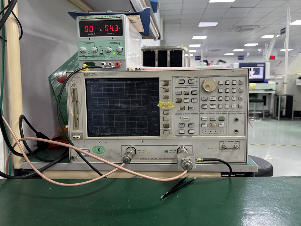
Choose a test for the failure mechanism and name its limits. Optical inspection can support visible assembly checks; it cannot establish receive-chain noise, shield effectiveness, or installed-line detection performance. A network analyzer characterizes a connected network’s frequency response under its setup conditions, while a powered functional fixture needs its own stimulus, acquisition settings, and pass criteria.
Separate prototype characterization from repeat production acceptance. During development, capture relevant supply, reference, and receive-channel behavior across agreed states. For production, select repeatable checks that detect the established failure risks without promising that a short fixture sequence reproduces every line disturbance. The requirement-led PCB test plan provides the broader method for assigning each requirement an evidence record.
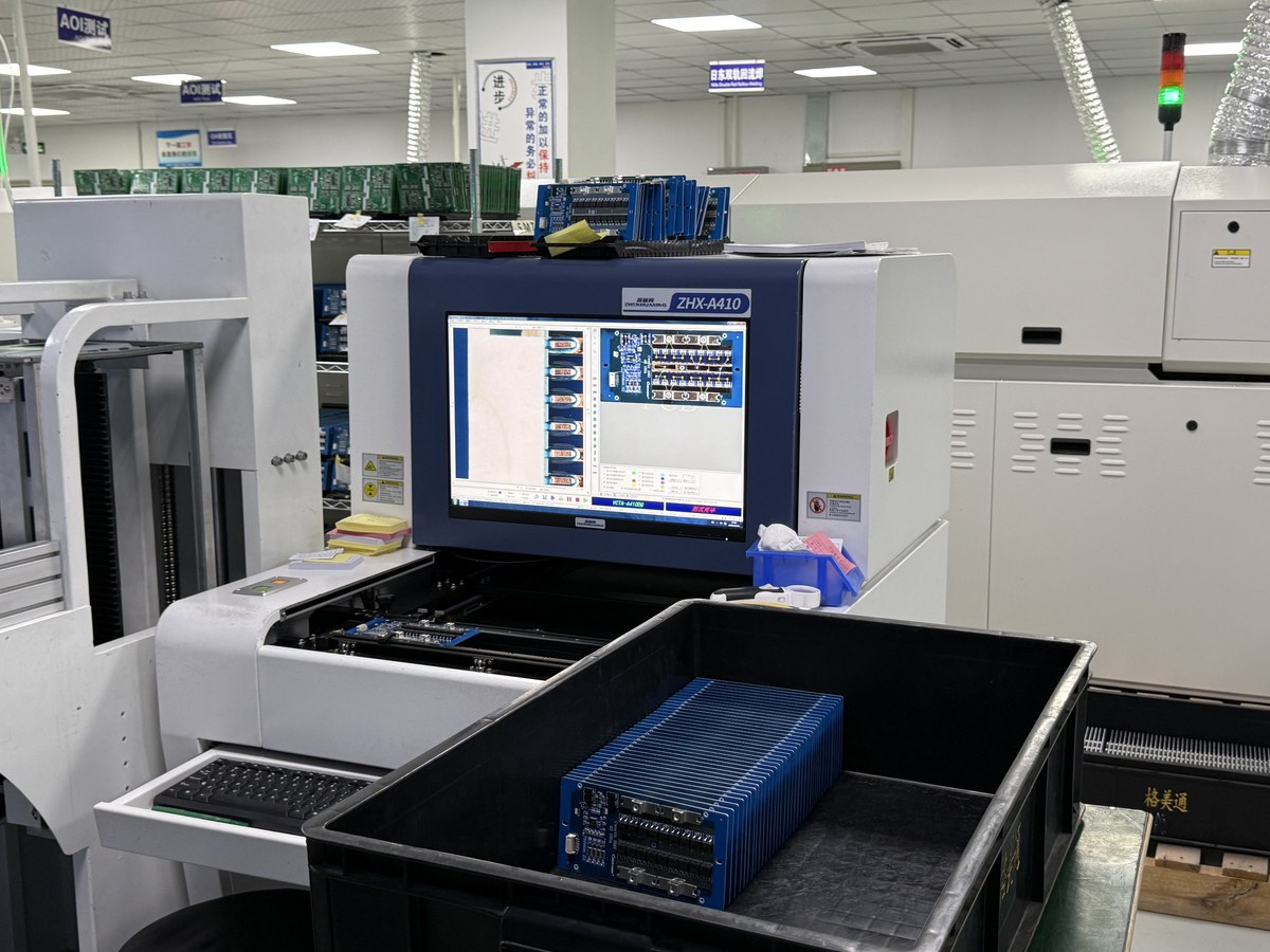
The official OrinewPCB AOI test clip shows the optical inspection process discussed here. Use it to distinguish visual assembly evidence from the electrical and machine-level checks, rather than as a demonstration of detector EMI performance.
Release the grounding assumptions with the PCBA build
Release one controlled package that connects the drawing, approved components, build process, fixture, and acceptance record. Otherwise, the quotation may cover a correctly assembled board while excluding the noise investigation or installed-machine validation that the buyer expected. The full-turnkey PCB assembly scope brings fabrication, component sourcing, and assembly together; project-specific electrical testing still needs an agreed definition.
| Controlled requirement | Release item | Acceptance boundary |
|---|---|---|
| Return paths and layer structure | PCB revision, stackup, routing data, grounding and mounting notes | Design/DFM review of the intended geometry, not a generic “good ground” statement |
| Receive-input network | Approved BOM and substitution restrictions for filters and protection | Component identity plus any required circuit characterization |
| Harness and chassis interface | Pinout, shield termination, isolation and assembly drawing | Agreed assembly checks; machine-owner approval of installation connections |
| Board functional performance | Fixture, firmware, stimulus, acquisition bandwidth and numeric limits | Repeatable board record tied to the tested configuration |
| Installed detection performance | Head/machine configuration, product conditions and approved validation procedure | System-owner acceptance; not inferred from the bare board or AOI result |
Approve the current paths and input behavior first, then preserve those decisions through sourcing and assembly. A stable bench board and a stable installed detector are related milestones with different evidence. For a production project, provide the controlled build package and test scope with Gerbers or ODB++, BOM, placement data, quantities, and fixture requirements so the combined PCBA work can be reviewed and its quoted boundaries made explicit.
Technical references accessed October 21, 2026. ADI’s return-current tutorial is dated October 15, 2012; LOMA’s metal-free-zone article is dated June 1, 2021. Apply the current component datasheets, detector installation manual, and approved product requirements to the actual design.
Latest Blog
Contact Info
Phone: +86-755-82882936
Email: [email protected]
WhatsApp: +86-13570802455
Wechat: +86-13570802455
Address: 2nd floor,D Bldg.,Electric Link Technology Bldg.,Gongming,Guangming New Dist.,518106 Shenzhen, China