
FR-4 vs Rogers vs PTFE: Select PCB Materials by Requirement
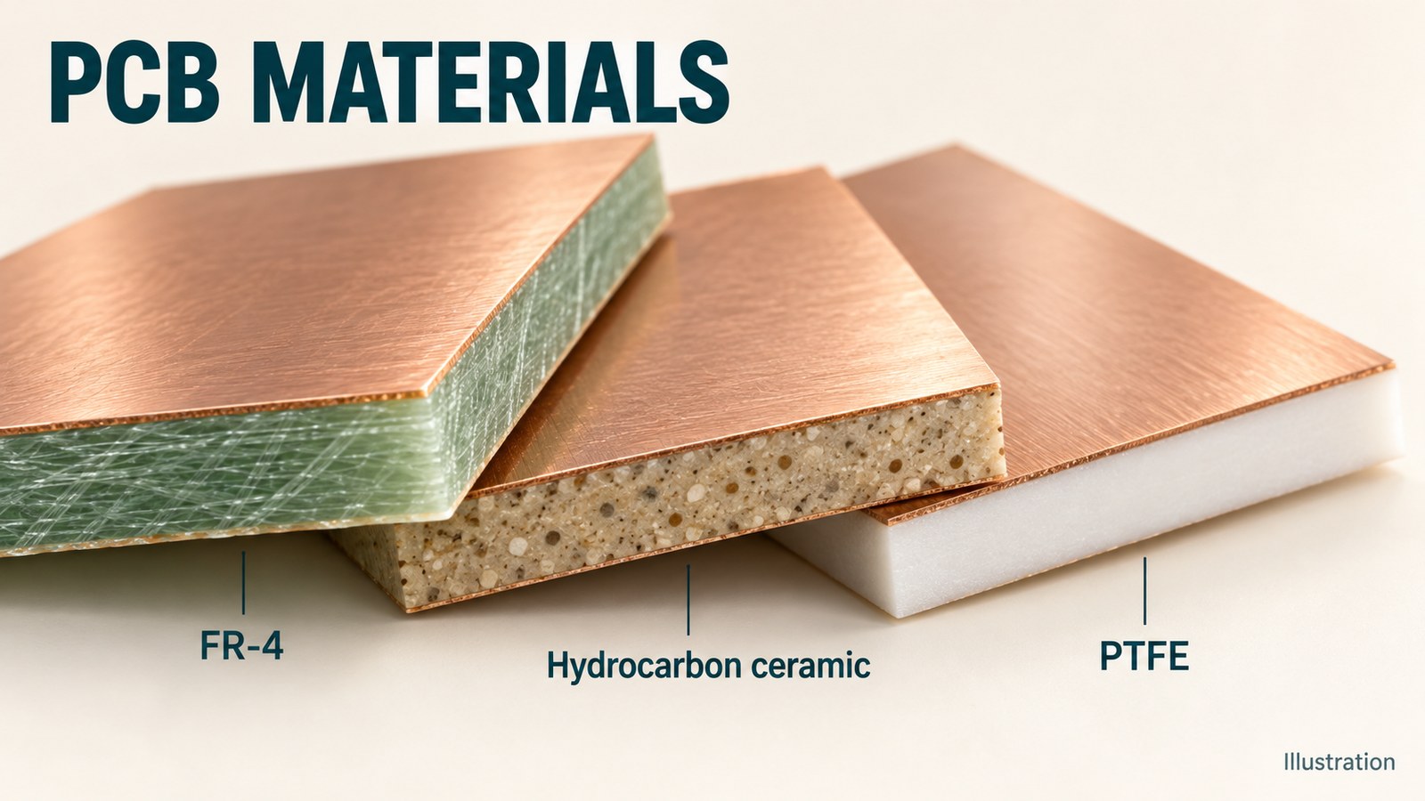
Table of Conent
Table of Conent
Choose a PCB laminate by the electrical margin and manufacturing evidence the finished board needs. FR-4 can be a suitable starting point when a specified glass-epoxy construction meets the loss, impedance, thermal, and reliability requirements. A hydrocarbon ceramic laminate can offer a useful route when tighter dielectric control or lower loss is needed with familiar fabrication processes. A PTFE composite may be appropriate when its verified electrical properties justify a different processing route.
The phrase FR-4 vs Rogers vs PTFE mixes a material grade, a manufacturer, and a polymer family. Rogers sells both PTFE and non-PTFE laminates. Compare exact grades, constructions, and test conditions; then qualify the stackup and assembly process. Neither a brand name nor an operating frequency alone establishes which material a board needs.
Compare material families, not a brand against a resin
Begin with a named material and its construction. “FR-4,” “Rogers,” and “PTFE” are incomplete purchasing specifications, even when they are convenient search terms.
FR-4 commonly describes glass-reinforced epoxy laminates, but one FR-4 product does not represent every resin system, glass style, or resin content. For example, Isola identifies 370HR as an FR-4 epoxy system. Its thermal and electrical data apply to that product and the stated measurement conditions, not to an unrestricted “FR-4 equivalent.”
Rogers RO4000 materials provide a different example: the manufacturer describes a hydrocarbon ceramic system that supports conventional epoxy/glass processing. Its RO3000 family uses ceramic-filled PTFE. A ceramic filler therefore does not tell you whether a laminate is PTFE-based, and the Rogers name does not specify the resin chemistry.
On a drawing or sourcing request, identify the manufacturer, grade, dielectric construction, thickness and tolerance, copper type, and permitted substitutions. The Rogers PCB fabrication scope is a relevant service reference, but any proposed grade and construction still need project-specific confirmation. A material listing is not evidence that every thickness, hybrid build, or RF acceptance test is available.
Start with the loss and phase budget
The controlling requirement should select the candidate material route. Establish what the complete interconnect must achieve before comparing laminate prices or adopting a frequency cutoff from a general guide.
For an RF path, define the frequency band, trace length, allowable insertion loss, return loss, phase tolerance, and operating environment. For a digital channel, include edge rates and the relevant channel bandwidth rather than relying only on the clock rate. Separate the board’s allocated loss from connectors, packages, cables, and other channel elements. A low-loss substrate cannot compensate automatically for a poorly controlled launch or reference-plane discontinuity.
| Controlling requirement | Candidate route to evaluate | Evidence needed before release |
|---|---|---|
| Specified channel loss is met by the proposed construction | Named FR-4 grade may be sufficient | Model or measurement covering actual length, geometry, copper, and frequency band |
| Dielectric loss or phase variation consumes the available margin | Compare controlled low-loss thermoset and PTFE grades | Applicable Dk/Df data, temperature behavior, and construction-specific simulation |
| RF routing shares a board with power and control functions | Evaluate a hybrid stackup against an all-RF construction | Bonding system, reference planes, transitions, balance, and qualification plan |
| Assembly heat or service cycling dominates the risk | Select by the complete thermal/mechanical requirement | Material expansion, thermal durability, via construction, and assembly exposure |
| Material availability threatens repeat builds | Keep the approved grade or qualify a documented alternative | Exact construction availability and electrical, fabrication, and assembly change assessment |
As a hypothetical example, a short RF connection and a long phase-sensitive feed network can have different substrate needs at the same operating frequency. First calculate or measure each path’s margin. If the candidate fails, determine whether dielectric loss, conductor loss, geometry, or a transition causes the failure. Changing the laminate addresses only part of that list.
When those requirements are defined, share the proposed stackup and assembly constraints with the fabrication files and build quantity so the material, manufacturability, and assembly assumptions can be checked together. Identify the RF paths requiring validation; do not assume that an assembly quotation includes RF characterization.
Normalize Dk and Df before comparing data sheets
Compare dielectric properties only after aligning the material grade, frequency, method, construction, and intended use of the number. Dielectric constant, or Dk, influences propagation and impedance; dissipation factor, or Df, describes dielectric loss under the stated conditions.
The following values are representative manufacturer data, not guaranteed finished-board acceptance limits. They illustrate why a one-line “FR-4 versus PTFE” property table can be misleading.
| Material and source | Published Dk | Published Df | Comparison limitation |
|---|---|---|---|
| Isola 370HR, data sheet dated April 15, 2021 | 4.04 at 2 GHz | 0.0210 at 2 GHz | Bereskin stripline entries; do not compare directly with a different frequency or method |
| Rogers RO4350B, RO4000 data sheet revised August 3, 2022 | Process: 3.48 ± 0.05 at 10 GHz/23°C; design: 3.66 over 8–40 GHz | 0.0037 at 10 GHz/23°C | Process Dk and Df use clamped stripline; design Dk uses differential phase length |
| Rogers RO3003, RO3000 data sheet revised January 30, 2024 | Process: 3.00 ± 0.04 at 10 GHz/23°C | 0.0010 at 10 GHz/23°C | Process entries use IPC-TM-650 2.5.5.5; confirm the applicable design input separately |
Sources: Isola 370HR data sheet, Rogers RO4000 data sheet, and Rogers RO3000 data sheet. Documents checked October 27, 2026.
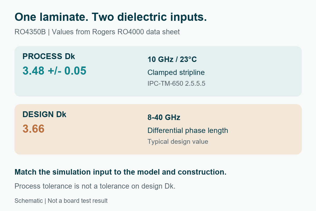
Do not transfer the ±0.05 process tolerance to the 3.66 design value. Confirm which input the field solver and transmission-line model require. Include dielectric spacing and copper geometry in the same model; a correctly named laminate with an incorrect pressed thickness still gives an incorrect prediction.
Source revisions also matter. On October 27, 2026, the RO3003 product-page table displayed a design Dk of 3.16, while its linked January 2024 data sheet listed 3.00. This discrepancy does not establish which value fits a particular design. Obtain the applicable manufacturer guidance, construction, and model basis before freezing a phase-sensitive layout.
Qualify the stackup and fabrication route
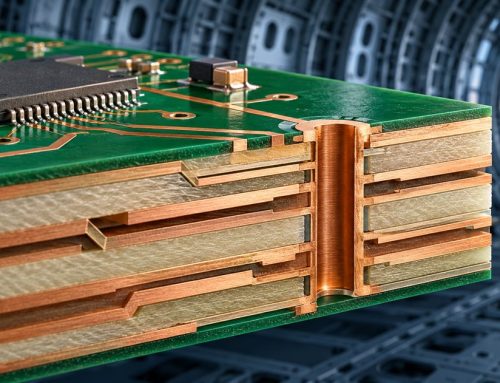
A laminate’s electrical benefit must survive the actual build. Qualify bonding layers, copper, drilling and hole preparation, layer registration, and assembly exposure as one construction.
PTFE processing deserves an explicit discussion. The Rogers RO3000/RO3200 fabrication guide requires treatment of drilled PTFE hole walls before conductive seed deposition and describes sodium or plasma approaches. It also distinguishes PTFE surface activation from desmear needed by some bonding systems. “We process Rogers” is therefore an insufficient answer to a question about a specific PTFE multilayer build.
Ask the fabricator which approved process covers the selected grade, bonding system, via geometry, and thermal exposure. Request the agreed evidence for hole quality and reliability. Keep these fabrication controls separate from finished assembly inspection and functional testing; an optical inspection result cannot demonstrate RF loss or plated-hole durability.
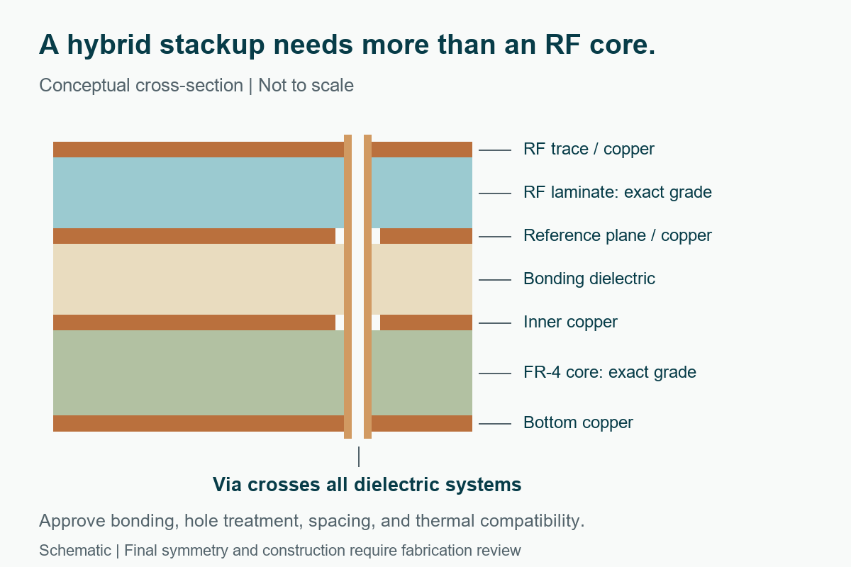
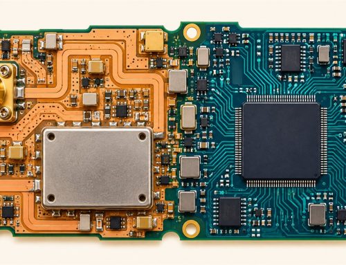
A hybrid build can concentrate the chosen RF dielectric where it is needed, but its cost advantage must be quoted rather than assumed. Bonding materials, additional processing, panel utilization, minimum purchases, and qualification work can change the result. Confirm the core, prepreg, and lamination controls, including pressed dielectric spacing and the compatibility of different layers.
Specify copper foil as well as nominal copper weight when the loss model depends on its surface profile. Review etched conductor dimensions, finish, mask exposure, connector transitions, and return paths. Compare candidate constructions using the same assumptions, then correlate the chosen model with an agreed coupon or prototype measurement. The required measurement method, fixture, calibration, limits, and responsibility belong in the test plan.
Release a material-specific fabrication and assembly package
Release an approved construction and acceptance plan, not a generic request for a “high-frequency PCB.” Procurement needs enough detail to recognize when an offered substitution changes the validated design.
Record the exact laminate and bonding grades, stackup revision, finished and dielectric thickness tolerances, copper specification, impedance requirements, and substitution policy. Attach the applicable data-sheet revisions and the model inputs used for release. If a supplier proposes an alternative, assess the electrical model, bonding and hole preparation, assembly exposure, and any required validation before approving it.
For assembled boards, connect that fabrication baseline to the BOM, approved component alternatives, placement data, assembly drawing, firmware/configuration where applicable, and inspection and test requirements. Use documented DFM dispositions to close deviations. A supplier’s stackup proposal should become part of the released record rather than remain in an email disconnected from the order.
Separate the qualification scope from recurring production acceptance. Identify who owns RF performance validation, what the fabricator supplies, and what assembly testing covers. A passed impedance coupon is useful evidence for its specified measurement; it does not automatically demonstrate insertion loss, antenna efficiency, or every assembled RF path.
The practical choice between FR-4, hydrocarbon ceramic, and PTFE is the least burdensome approved construction that meets the complete requirement with adequate margin. Preserve its material identity, process conditions, and validation evidence through sourcing changes and repeat builds.
For a complete PCBA project, provide the controlled fabrication and assembly package with the BOM, placement files, quantity, material restrictions, test responsibilities, and delivery target. That gives OrinewPCB a defined basis for confirming the fabrication, component sourcing, assembly, and test scope before quotation.
Latest Blog



Contact Info
Phone: +86-755-82882936
Email: [email protected]
WhatsApp: +86-13570802455
Wechat: +86-13570802455
Address: 2nd floor,D Bldg.,Electric Link Technology Bldg.,Gongming,Guangming New Dist.,518106 Shenzhen, China