
77 GHz Radar PCB Design: Separate Array Pitch from RF Tolerances
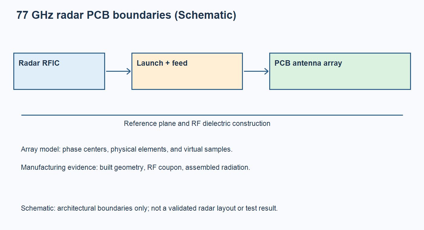
Table of Conent
Table of Conent
77 GHz radar PCB design requires separate controls for antenna phase-center positions, guided RF feed paths, and the evidence used to accept the finished assembly. Start with the array model and the selected radar device’s reference design, then establish the stackup and obtain fabrication feedback before freezing dimensions. A half-wavelength spacing calculation alone cannot specify patch geometry, feed routing, or a manufacturing tolerance.
At 77 GHz, the free-space wavelength is approximately 3.89 mm. Half of that is about 1.95 mm, but this is a reference for certain array-sampling arrangements, not a universal pitch for every patch or transmit antenna. Feed-line phase depends on propagation through the actual PCB structure. For an OEM releasing a board with PCB antennas, the practical task is to connect each sensitive feature to a design-derived allowance, an agreed manufacturing control, and a verification method. Antenna-in-package devices require their own package and board guidance.
Identify which antenna spacing the drawing controls
Label the array coordinates before dimensioning the antenna artwork. Physical patches within a series-fed antenna, the phase centers of separate receive channels, and the samples of a MIMO virtual array describe different things. A dimension labeled only “antenna pitch” leaves room for a costly interpretation error.
TI’s MIMO radar application report explains arrival-phase differences and how transmit and receive coordinates form a virtual array. In a simplified far-field example, put two transmit phase centers at 0 and 4d, and four receive phase centers at 0, d, 2d, and 3d. Their coordinate sums produce eight virtual positions from 0 through 7d. The transmit separation is 4d even though the virtual samples are spaced by d.
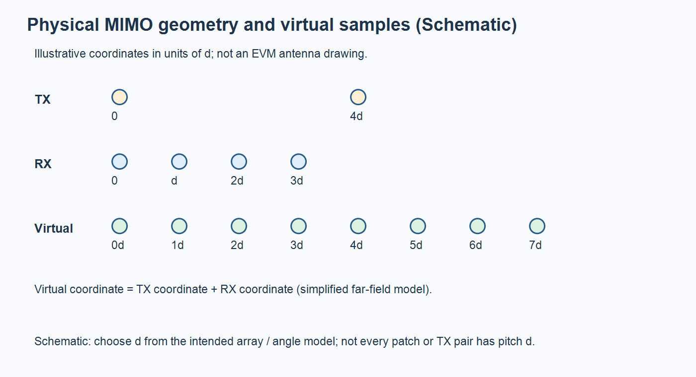
Choosing d near half the free-space wavelength is useful in a simple uniform array intended for a broad unambiguous angular field. It does not settle element patterns, mutual coupling, elevation behavior, or the channel mapping used by the estimator. Record those assumptions alongside the coordinates.
Use a device reference as a complete starting configuration. The IWR1843BOOST antenna reference provides layout and stackup information and explicitly labels its radiation patterns as simulated. Copying an outline while changing the substrate or enclosure does not reproduce that reference configuration or establish measured performance.
Carry the RF stackup into the package launch and feed
Release the RF layer construction together with the antenna and launch geometry. A nominal “50-ohm line” describes only part of the path from a radar package to a radiating element. The transition, reference-plane openings, nearby metal, and dielectric construction also belong to the RF model.
Rogers’ millimeter-wave material guidance discusses the effects of material properties, copper roughness, and conductor and dielectric dimensions on loss and phase. Accordingly, a purchasing description containing only a laminate family and overall board thickness is insufficient to freeze propagation conditions.
Identify the exact RF material construction, dielectric thickness, copper and foil requirements, finish, and any solder-mask openings in the released package. Separate nominal material data from the values and conditions used in simulation. A substitute with a similar headline dielectric constant still needs an engineering assessment of the properties that matter to this design.
Ask the fabricator to identify differences between the proposed build and the modeled construction before tooling. If an RF stackup changes, return the launch and feed to the design owner for review. This approval step is less expensive to resolve while the data can still be changed than after assembly produces an unexplained channel difference.
Turn phase sensitivity into a design-specific tolerance budget
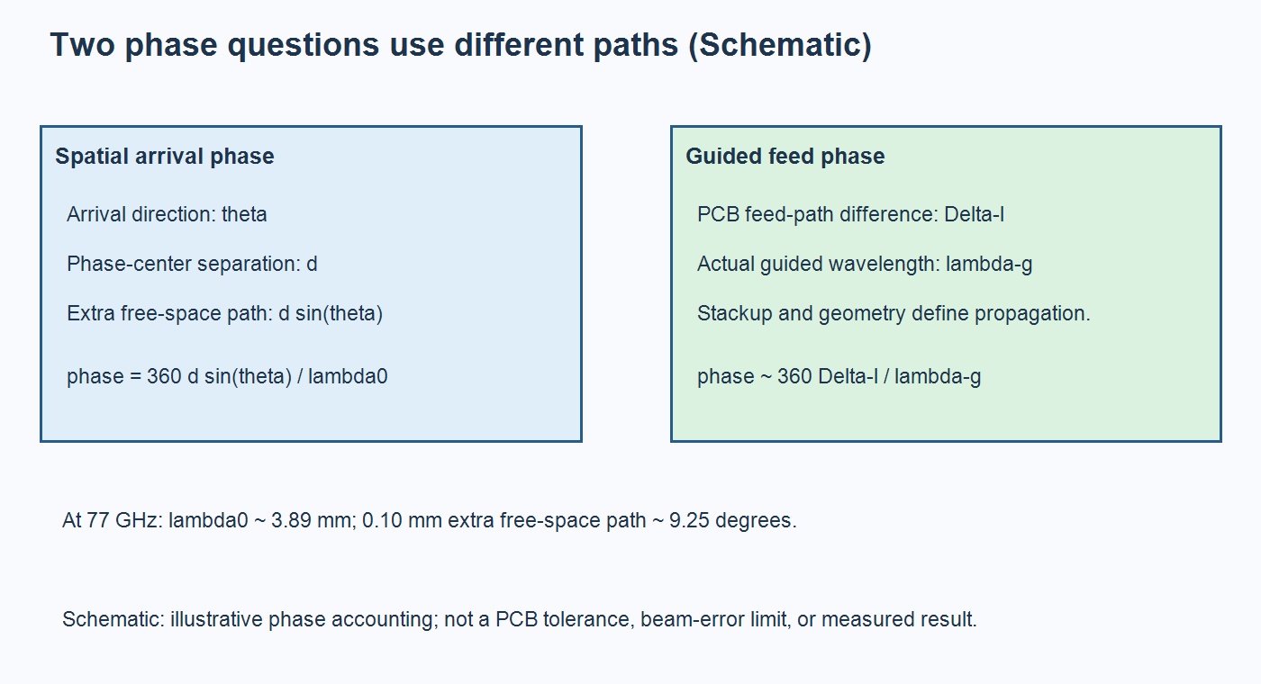
Use the wavelength appropriate to the path being evaluated. For antenna phase centers separated by d, a simple plane-wave arrival model gives a spatial phase difference of 360d sin(theta)/lambda-zero degrees. A guided feed-path difference instead gives approximately 360 delta-l/lambda-g degrees, where lambda-g is the guided wavelength of that structure.
For scale, dividing the speed of light by 77 GHz gives about 3.893 mm. An additional 0.10 mm of free-space travel corresponds to approximately 9.25 degrees of phase. This calculation is neither an allowable etch error nor a prediction of beam-angle error. In a PCB feed, use the modeled propagation behavior; substituting free-space wavelength or a nominal bulk dielectric constant can answer the wrong question.
For an initial manufacturing review, share the RF stackup and critical geometry package with OrinewPCB, together with the dimensions that require design-owner approval before any adjustment. That gives the fabrication and assembly discussion a defined technical starting point.
Build the budget around the intended operating band, channel relationships, and acceptance targets. Sweep plausible fabrication variations in the RF model and identify which combinations threaten those targets. Do not turn a single nominal-frequency result into a universal micron or degree requirement. Calibration assumptions also need an owner: a measured channel correction is not permission to leave geometry or assembly changes uncontrolled.
Specify RF geometry and CAM change authority
State which RF features are fixed and who may approve changes. An instruction to achieve controlled impedance can otherwise conflict with an instruction to reproduce antenna or launch artwork. Separate routine manufacturability questions from proposed changes to modeled RF geometry.
TI’s RF PCB design and manufacturing guide, published in 2018, recommends deriving dimensional tolerances through electromagnetic parameter sweeps and addresses coordination with the board manufacturer. Its device examples are useful references, not universal dimensions for every current radar product.
The following release matrix is a practical way to turn that design work into reviewable instructions. Populate the allowances from the actual design analysis and the fabricator’s proposed process; the table deliberately provides no generic tolerance values.
| Controlled item | Record before release | Approval question |
|---|---|---|
| Array coordinates | Phase-center definition, datums, channel labels, and intended virtual mapping | Does the artwork match the array model and firmware mapping? |
| Package launch and RF feeds | Critical widths, gaps, plane openings, and modeled layer construction | Which dimensions may CAM change, and which require RF review? |
| RF dielectric and copper | Approved construction, property basis, foil requirements, and proposed variation | Does the proposed build remain inside the evaluated design space? |
| Mask, finish, and nearby metal | Defined openings and exclusions with explicit drawing references | Would a process adjustment change the modeled RF environment? |
| Inspection evidence | Feature, datum, method, sample plan, and report requirement | Can the agreed measurement resolve the specified allowance? |
Keep each proposed deviation tied to a drawing revision and a named approver. The impedance-controlled PCB RFQ guide describes the broader stackup and coupon approval boundary. For this radar release, add the antenna and launch features that an impedance-only review would leave unresolved.
Separate fabricated geometry, RF coupons, and radiated acceptance
Accept each result only for the property it actually measures. A dimensional report, a transmission-line coupon, and an assembled radar test address different questions. Passing one does not automatically establish the others.
| Evidence | Decision it supports | Boundary to keep explicit |
|---|---|---|
| Fabricated-feature inspection | Whether specified widths, gaps, registration, or construction match the drawing within the agreed method | Geometry alone does not measure antenna pattern or radar performance. |
| Defined RF coupon or test structure | The electrical behavior of that structure under its stated frequency range, fixture, and calibration | A coupon does not include every package transition, antenna, enclosure, or assembled channel. |
| Assembled radiated or system test | Whether the configured unit meets the selected RF or application acceptance criteria | Results apply to the tested configuration, setup, processing, and stated conditions. |
A conventional impedance coupon can support an agreed impedance check. It does not, by itself, demonstrate antenna gain, channel phase balance across the operating band, or detection performance. If a separate RF structure is required, define its purpose, interfaces, measurement range, calibration, and correlation to the production board before assuming it closes that gap.
For assembled validation, identify the actual housing or radome configuration, fixture, firmware, calibration state, and operating conditions. Distinguish a bare-board acceptance gate from an assembled-unit gate and a final application test. When a result fails, that separation helps the team investigate the relevant boundary instead of attributing every discrepancy to laminate or etching.
Agree where each test will occur, who supplies the fixture and reference data, and who approves the report. Specialized millimeter-wave measurement is a project-specific scope to confirm, rather than an implied inclusion in a standard PCB assembly order.
Release the radar assembly with a defined verification scope
Release fabrication data, assembly data, and acceptance responsibilities as one controlled configuration. Include the RF drawings and stackup, BOM, placement files, assembly instructions, approved deviations, programming requirements, and test specifications. Identify the revision used for any simulated or measured baseline.
Apply the BOM alternate approval workflow to proposed component substitutions and document who assesses their effect on the released unit. An approved purchasing alternate and a validated RF configuration are separate decisions that need to remain traceable.
OrinewPCB’s full-turnkey PCB assembly scope connects board fabrication, component sourcing, and assembly. Define any radar-specific modeling, RF measurement, calibration, or system validation separately with the responsible parties; do not infer those deliverables from the assembly scope.
When preparing the build inquiry, provide the released radar assembly files and verification requirements so OrinewPCB can review the manufacturing package and clarify sourcing, assembly, and test responsibilities before production.
Latest Blog
Contact Info
Phone: +86-755-82882936
Email: [email protected]
WhatsApp: +86-13570802455
Wechat: +86-13570802455
Address: 2nd floor,D Bldg.,Electric Link Technology Bldg.,Gongming,Guangming New Dist.,518106 Shenzhen, China