
Aluminum MCPCB Thermal Design: Specify the Dielectric and Heat Path
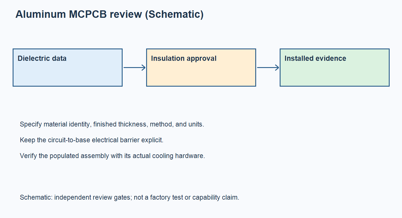
Table of Conent
Table of Conent
An aluminum MCPCB transfers heat through an electrically insulating dielectric before the heat reaches the metal base. Specify the dielectric material and finished thickness together, then evaluate the entire route to the heatsink and ambient. A high conductivity number alone cannot establish the operating temperature. For a first comparison, a uniform layer has thermal resistance approximately equal to thickness divided by conductivity and effective heat-transfer area; that estimate does not include lateral spreading or contact losses.
The practical decision is whether a proposed construction meets the temperature and insulation requirements in the installed assembly. This guide develops a comparison worksheet for aluminum insulated metal substrate (IMS) boards, separates material data from assembly evidence, and identifies the changes that require another review. It applies to a conventional insulated construction; a direct thermal path, multilayer IMS, or special via structure needs its own approved section.
Define the heat path before choosing a dielectric grade
Start with the device loss and temperature limit, and identify every interface through which that heat must travel. A conventional single-circuit-layer aluminum MCPCB contains circuit copper, an insulating dielectric, and an aluminum base. The base spreads heat after it crosses the dielectric; it does not remove the insulation layer from the thermal path.
Draw the path from the device thermal pad through solder, copper, dielectric, base, thermal interface material (TIM), and heatsink. Mark the temperature reference points used by the component manufacturer. Do not substitute a measured board temperature for junction temperature without the package-specific relationship and its applicable conditions.
Record the worst intended operating states, including simultaneous heat sources, enclosure ambient, airflow, and heatsink mounting. Distinguish electrical input power from heat dissipated in the device. The chosen loss model should state what is included, especially for LEDs that also emit optical power. Keep uncertain losses visible as assumptions rather than hiding them inside an apparently precise result.
The site’s aluminum PCB manufacturing overview identifies the service category. It is a starting point for feasibility discussions, not approval of a particular laminate, insulation barrier, or thermal performance target.
Compare thickness and conductivity on the same area basis
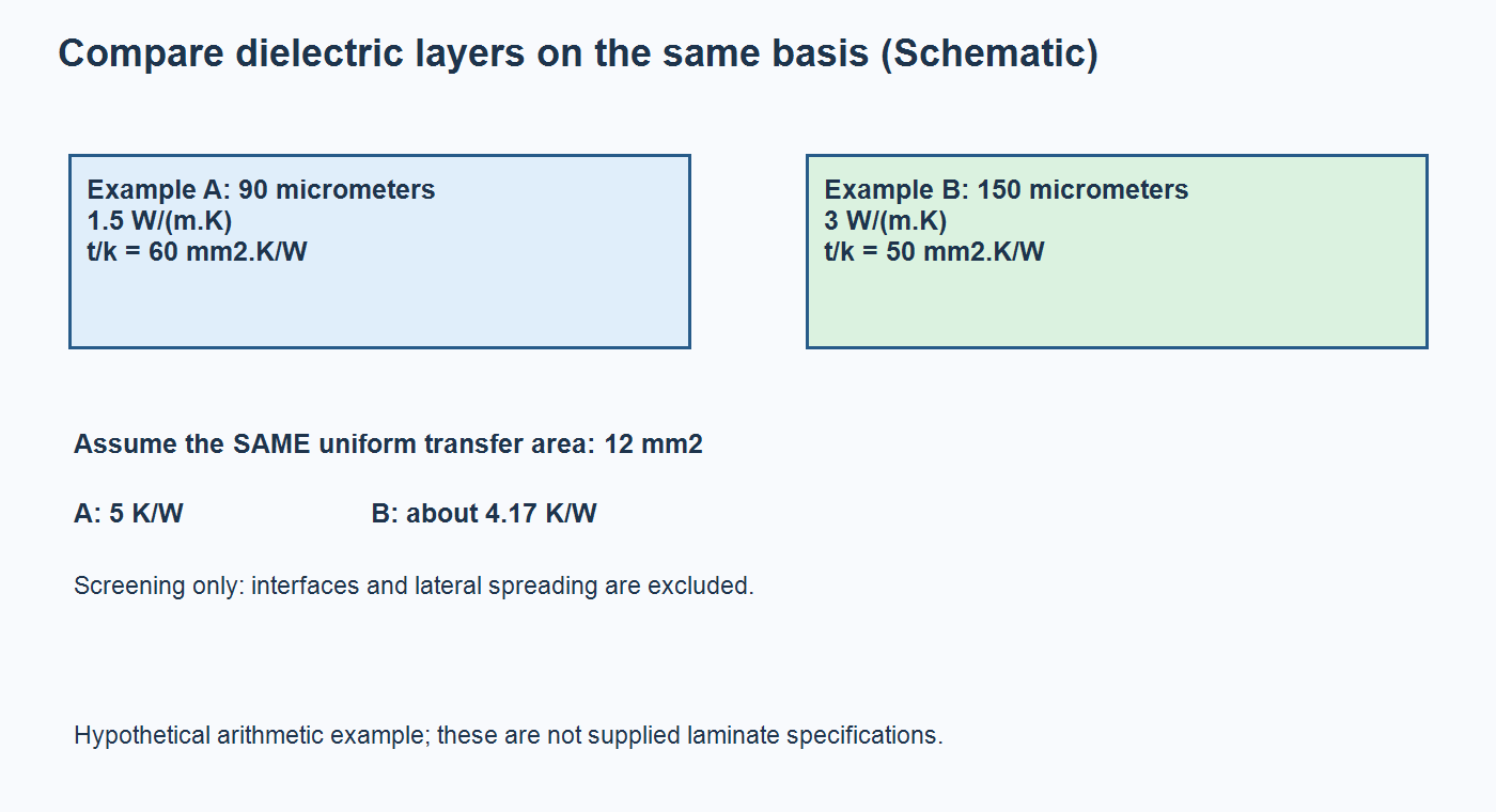
Use R = t/(k × A) only as a one-dimensional screening model for a uniform layer. Here, R is in K/W, t is thickness in meters, k is through-thickness conductivity in W/(m·K), and A is the assumed transfer area in square meters. A temperature difference of one kelvin has the same magnitude as one degree Celsius.
For an explicitly hypothetical example, compare dielectric A at 90 µm and 1.5 W/(m·K) with dielectric B at 150 µm and 3 W/(m·K). Their area-normalized values, t/k, are 60 and 50 mm²·K/W respectively. Over an assumed 12 mm² uniform area, the layer estimates are 5 and about 4.17 K/W. The thicker material can have the lower calculated resistance because conductivity and thickness change together.
These are arithmetic examples, not available OrinewPCB materials or acceptance limits. They exclude interfaces and spreading. Do not use the entire board area merely because the base is metal; identify the local area assumption and test how the conclusion changes when it is reduced. A large heatsink footprint cannot automatically be assigned to the dielectric directly beneath a small heat source.
Request comparable evidence before approving a substitution
Approve a dielectric using its identified construction, electrical requirements, and comparable thermal data. Catalog conductivity, area-normalized impedance, and finished-assembly thermal resistance answer different questions. Keep their units and test boundaries attached to every value.
Henkel’s THERMAL CLAD selection guide explains that conductivity comparisons depend on dielectric thickness, area, and interfacial resistance, and that different measurement methods can produce different results. Request the method and construction behind the proposed value. A larger headline number measured differently is insufficient evidence for an equivalent replacement.
| Decision | Record for each candidate | Hold approval when |
|---|---|---|
| Thermal screening | Material code, finished thickness and tolerance, conductivity direction and method, assumed area | Values describe different layers, units, or unreported test conditions |
| Insulation | Circuit-to-base boundary, applicable product requirements, agreed test and acceptance criteria | A material breakdown value is treated as a complete product isolation rating |
| Assembly performance | Device losses, populated revision, solder attachment, TIM, heatsink, mounting and ambient | The proposed stack is compared under different cooling or operating conditions |
| Repeat production | Approved laminate identity, substitution rules, inspection records and change owner | A replacement changes the reviewed construction without engineering approval |
If candidate materials remain open, share the dielectric comparison and thermal boundary drawing with the voltage requirements, heat-source map, and build quantity so feasibility and quotation assumptions can be reviewed together.
Keep insulation approval separate from thermal screening
A lower calculated thermal resistance does not authorize a thinner electrical barrier. Establish which circuit nodes must remain isolated from the base, accessible hardware, and chassis, then have the responsible product engineer define the applicable insulation requirements.
A material’s published breakdown result is not interchangeable with continuous working voltage or a finished product’s dielectric withstand test. Thickness variation, exposed edges, holes, fasteners, contamination, and the complete insulation architecture can affect the review. Request the supplier’s data for the actual material and construction rather than interpolating an allowable voltage from thickness alone.
Use the PCB hipot insulation-path guide to organize the boundary and test-access questions. The approved plan should identify the conductors on each side, product state, test conditions, acceptance criteria, and responsible party. Changing the dielectric may require both thermal and electrical reapproval; passing either evaluation does not establish the other.
Treat the board-to-heatsink interface as a separate design variable
Control the TIM and mounting arrangement when comparing board materials. Otherwise, an apparent dielectric improvement may actually reflect a different contact condition, or disappear when the board is installed in its enclosure.
In its June 2019 FR-4 and IMS GaN inverter comparison, Texas Instruments documents how mounting and contact affected the TIM choice and thermal results. The tested boards, interface materials, and geometry differ; its outcome is not a universal aluminum-to-FR-4 improvement factor.
For a project review, identify the contact land, surface condition, permitted flatness variation, TIM identity and application, hardware, and approved fastening procedure. Ask who supplies and installs each item. If the board supplier quotes only fabrication, do not assume the final contact assembly is included in its thermal evidence.
When evaluating a hotter sample, change one controlled variable at a time. First confirm load, ambient, and measurement locations. Then compare contact and assembly condition before attributing the difference to dielectric conductivity. Preserve the original mounting record so the investigation can distinguish construction variation from an installation change.
Verify the populated assembly under representative conditions
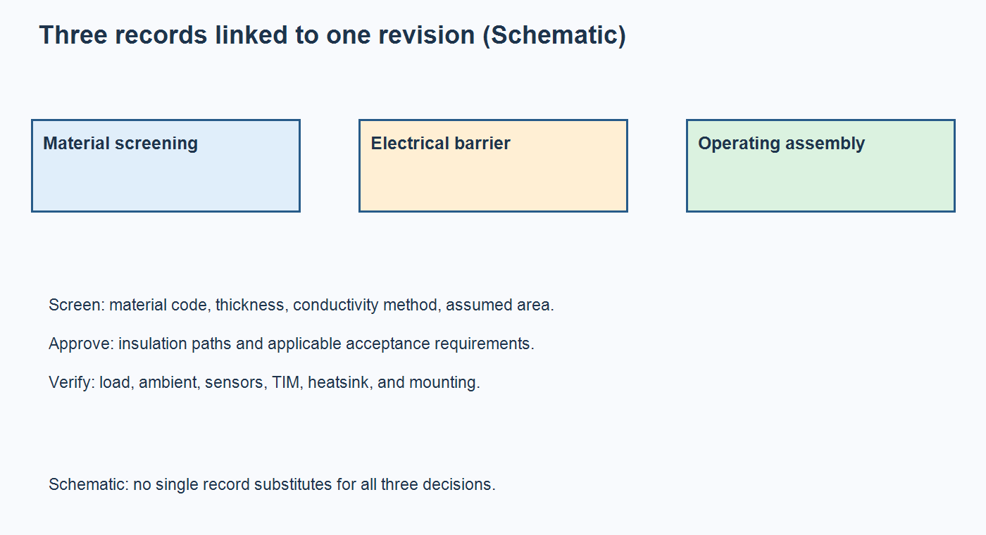
Accept the thermal design using measurements tied to the actual operating assembly and stated limits. A bare-board material certificate or an image of a cool heatsink cannot establish the hottest component’s temperature.
Cree LED’s PCB thermal performance guide, revision 4A, recommends verification under real operating conditions and describes measurements near the LED thermal pad, on the heatsink, and in ambient air. Use the measurement method appropriate to the selected device; its LED-specific layouts and results are not generic MCPCB design rules.
Write the verification record before building samples: board and BOM revision, losses or operating mode, enclosure and heatsink revision, airflow, sensor locations and attachment, stabilization criterion, limits, and disposition. Record instrument limitations and the method used to estimate junction temperature. Compare candidates using the same basis, and explain any unavoidable difference.
Assembly process verification has a different purpose. The thermocouple placement guide for reflow profiling addresses soldering exposure on a populated board; it does not replace powered thermal validation. Keep those records separate even when both use temperature sensors.
Define change triggers as part of acceptance. A new dielectric family, finished thickness, package thermal pad, solder attachment, TIM, fastening method, or operating load can change the result even if the board outline stays unchanged. Assign an engineer to decide whether existing evidence remains applicable. Procurement should retain the approved material code and revision in the repeat-order record, and request review before accepting a substitute. This makes a later temperature comparison traceable to the construction that was actually purchased rather than merely to a supplier name.
Release one construction and one assembly scope
Freeze the material identity, dielectric thickness, drawing revision, and acceptance responsibilities before comparing final prices. A procurement line that says only aluminum PCB leaves essential assumptions unresolved.
Provide fabrication data, the dimensioned stack and outline, BOM, placement file, assembly drawing, quantities, permitted alternatives, and thermal and insulation requirements. Include TIM and heatsink details when they affect the supply scope. The full-turnkey PCB assembly scope connects fabrication, component sourcing, assembly, and testing; confirm the project-specific construction and test ownership with OrinewPCB.
An aluminum base is justified when the controlled assembly meets its temperature limits while preserving the required electrical barrier. For a released project, provide the manufacturing files and installed test requirements with the approved dielectric and cooling hardware so the team can assess fabrication, sourcing, assembly, and the requested verification scope on a consistent basis.
Latest Blog
Contact Info
Phone: +86-755-82882936
Email: [email protected]
WhatsApp: +86-13570802455
Wechat: +86-13570802455
Address: 2nd floor,D Bldg.,Electric Link Technology Bldg.,Gongming,Guangming New Dist.,518106 Shenzhen, China