
Mode S Transponder PCB: Release the Stackup and RF Test Boundary
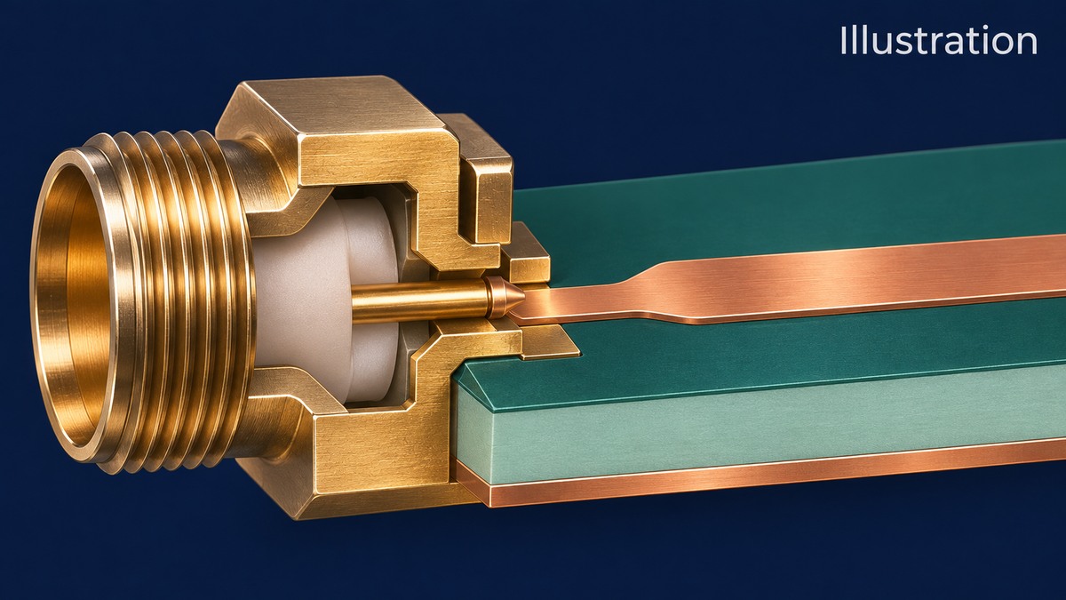
Table of Conent
Table of Conent
A Mode S transponder PCB stackup should be released as a controlled construction and measurement agreement. Specify the actual materials, layer relationships, finished geometry, reference planes and acceptance methods. Then identify which evidence comes from a fabrication coupon, which comes from the assembled radio-frequency (RF) path, and which belongs to equipment qualification. A passing impedance coupon does not establish that a connector launch, populated signal chain or complete transponder meets its requirements.
The original equipment manufacturer (OEM) owns those requirements and approves changes. The fabricator and assembler need enough controlled information to build repeatably and return evidence with a defined meaning. Start there rather than buying a generic “DO-160-qualified stackup.”
Define the qualification boundary before choosing layers
Equipment environmental qualification and PCB manufacturing acceptance answer different questions. The RTCA description of DO-160 concerns environmental conditions and test procedures for airborne equipment. It does not prescribe a universal transponder layer count, laminate, impedance tolerance or via construction. The equipment program must identify its applicable document revision, categories, configuration and performance criteria.
First establish the board’s role. A transponder can distribute RF, processing, power and interfaces across separate assemblies. A digital board receiving an already conditioned signal does not necessarily need the same construction as a board carrying a sensitive RF input or an output matching network. Mark the actual critical paths on the released layout instead of assigning one material to everything because the product operates in aviation.
Give each path an owner and a verification boundary. Identify the intended interface, controlled geometry, relevant operating conditions, measurement method and acceptance authority. A material certificate, a bare-board test and an assembled RF measurement should each support a named requirement. If the program needs environmental support from the manufacturer, specify the supporting records separately from the OEM’s equipment-level approval.
Keep the board’s manufacturing class and customer requirements explicit in the purchase package. Neither an application label nor an environmental test title supplies missing fabrication limits. Resolve responsibility for deviations before ordering material, particularly when a proposed alternate could affect the approved construction.
Close construction assumptions before CAM release
A useful stackup connects the circuit model to a buildable cross-section. Release layer order, reference planes, dielectric construction and finished thicknesses, copper definition, controlled trace geometry, surface finish and any solder-mask assumptions affecting the model. State whether dimensions describe artwork, etched copper or finished plated features. Otherwise, a fabricator can satisfy one interpretation while the designer calculates another.
The Rogers RO4000 data sheet distinguishes process and design dielectric values and cautions that typical properties are not specification values. Record which dielectric constant, or Dk, the circuit model uses, its source and the applicable construction. A material’s process-control number should not silently replace the model input. Equally, a modeled value should not become a receiving-inspection limit without an agreed basis.
| Decision | Released input | Evidence or approval needed |
|---|---|---|
| Material and dielectric model | Exact grade, construction, Dk basis and permitted alternatives | Fabricator confirms availability; design owner accepts the model and any substitution |
| Trace and reference relationship | Finished width, copper definition, dielectric separation and reference layer | Agreed field-solver construction and coupon geometry |
| Surface and conductor assumptions | Foil designation, finish and relevant mask treatment | Recorded manufacturing proposal and impact assessment |
| Fabrication adjustment | Allowed adjustment scope and approval route | Approved final stackup and CAM exceptions before panel release |
Material selection also needs a loss budget. AMD’s UG863 material comparison illustrates that insertion loss depends on more than a laminate label, including conductor characteristics and geometry. Its example values concern its stated constructions; they are not predictions for a Mode S board. Compare actual candidate constructions with the transponder’s path requirements rather than importing a cost multiplier or loss figure.
The impedance-controlled PCB RFQ requirements provide the general fabrication inputs. For this board, add the RF path identifiers and the boundary between a uniform line and each transition. An RF connector footprint, layer change or matching element can require a separate review from the line cross-section.
When these assumptions are documented, share the proposed construction and RF constraints with the fabrication files, assembly access needs and intended measurement scope. The review can identify material availability, geometry adjustments and test-access questions before a quotation fixes assumptions that engineering has not approved.
Separate coupon impedance from assembled RF acceptance
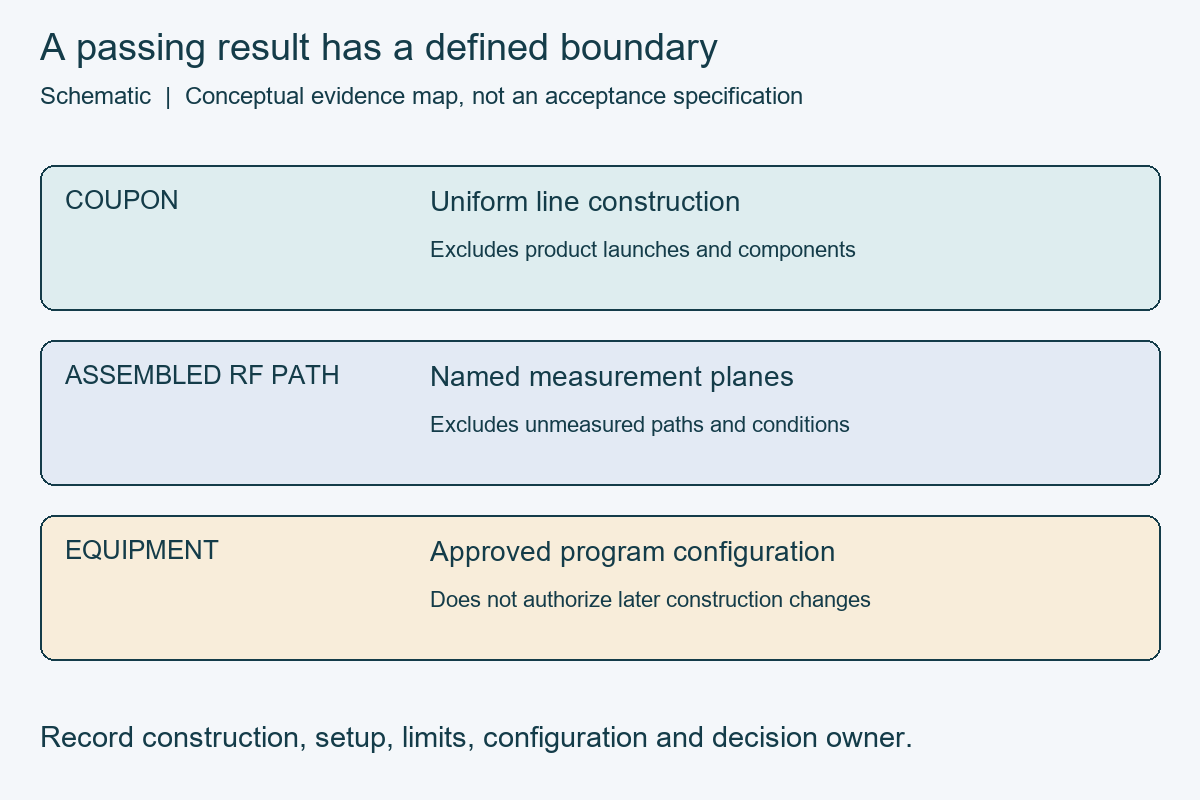
A uniform coupon demonstrates the behavior of its represented transmission-line construction under the agreed measurement method. It does not automatically include the product’s connector launch, component pads, vias, solder joints or matching network. Put that exclusion in the acceptance plan so a coupon pass is not used to close an unrelated RF discrepancy.
Define measurement reference planes for the assembled path: the locations at which the result is considered to begin and end. Specify the fixture and connection method, calibration or verification requirements, frequency range, operating state and handling of fixture contributions. If a reported result excludes part of the physical setup, record how that exclusion was established. Results with different included paths are not directly comparable merely because they share a unit.
| Evidence | What it can address | What remains outside the result |
|---|---|---|
| Fabrication impedance coupon | The specified uniform geometry and represented layer construction | Product launches, populated components and complete equipment behavior |
| Defined assembled RF path | The contracted path between named measurement planes in a recorded configuration | Unmeasured interfaces and untested operating or environmental conditions |
| Equipment environmental evaluation | Equipment performance under the approved program conditions | Unapproved construction changes or claims beyond the tested configuration |
The Rogers discussion of copper foils explains that conductor roughness can affect RF loss in a frequency- and construction-dependent way. Treat a foil change as an engineering input, not just a purchasing detail. The correct response is to compare the changed construction against the path budget and approved evidence, rather than declare every smoother foil necessary or every replacement equivalent.
Agree how failures will be separated. A coupon discrepancy can trigger construction and measurement review. A populated-path discrepancy may also involve connector installation, component population, fixture repeatability or calibration. Preserve the original result and configuration while investigating; widening a limit or repeating connections until a pass appears destroys useful diagnostic evidence.
If the program compares measurements before and after environmental exposure, preserve the same path definition and record any reconnection or fixture change. Otherwise, an apparent shift may reflect a different setup rather than a changed board. Define the comparison method and disposition owner in advance, including how an inconclusive result is reported. A missing measurement should remain an open requirement instead of being inferred from another passing test.
Preserve access and records through assembly
Assembly planning should protect the RF measurement boundary established during design. Identify connector seating, shield attachment, ground contacts, component orientation and any assembly operations that affect access. State which tests occur before shields, coating or enclosure installation, and which checks must occur after those operations. An inaccessible test point is a design and process decision, not a problem to discover after the first build.
The general manufacturing sequence in the official OrinewPCB video provides context for how a board moves through production. It does not show a qualified Mode S product or prove a particular RF acceptance process. Use the actual project traveler and contracted inspection plan to identify the records required for this assembly.
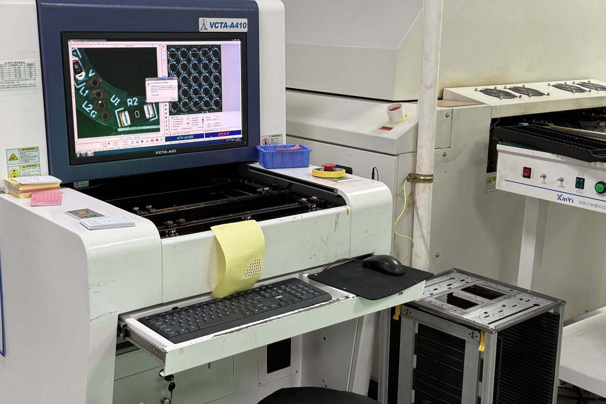
Connect each result to a physical board or agreed build lot, bare-board revision, assembly revision, fixture revision and test-program version. If programming is included, record the approved image identity separately. Define the traceability granularity and record retention contractually. A generic pass label cannot establish which construction, limits or component population produced the result.
Keep changes tied to RF and equipment evidence
A changed laminate, foil, dielectric thickness, finish, connector or fabrication route needs an impact decision against the released baseline. List the affected paths, the evidence that remains applicable and the checks that must be repeated. The design authority should approve that scope before the changed build proceeds. A passing earlier lot does not qualify a later construction by association.
The FAA’s AC 21-16G, issued in June 2011, describes environmental testing as a laboratory demonstration of equipment performance and explicitly separates it from a service-life measure. Keep that limited meaning in release discussions. The program determines the applicable qualification basis; a supplier should not infer flight eligibility from board-level production evidence.
Coordinate construction changes with Mode S component sourcing and change control. A new RF part can affect the same measurements as a changed board material. A full-turnkey PCB assembly scope can align fabrication, sourcing, assembly and specified testing around one approved configuration, while equipment approval stays with the responsible program.
The release decision is complete when the physical construction, model assumptions and measurement boundaries agree. For a project at that stage, provide the released fabrication and assembly package with the stackup, manufacturing files, bill of materials, placement data, quantities, approved alternates, RF path definitions and acceptance plan. These inputs let the quotation review separate contracted manufacturing evidence from remaining design and equipment-qualification work.
Latest Blog




Contact Info
Phone: +86-755-82882936
Email: [email protected]
WhatsApp: +86-13570802455
Wechat: +86-13570802455
Address: 2nd floor,D Bldg.,Electric Link Technology Bldg.,Gongming,Guangming New Dist.,518106 Shenzhen, China
