
RFID Reader PCB Tuning: Match the Antenna for ISO 14443
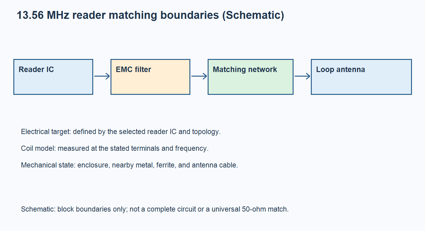
Table of Conent
Table of Conent
RFID reader PCB antenna matching starts with the selected reader IC, the measured loop, and the intended mechanical assembly. For a 13.56 MHz ISO/IEC 14443 reader, characterize the coil, calculate the matching network for the IC’s specified interface, and verify the populated reader in its enclosure. A resonance near the carrier frequency or a deep dip on a network analyzer does not, by itself, demonstrate reliable card communication.
Keep three results separate: the isolated coil model, the impedance of the assembled antenna network at the reader terminals, and powered reader performance. Each answers a different question. This guide covers HF magnetic-loop readers, rather than UHF RFID antennas or passive-tag chip matching. Its practical output is a repeatable tuning record that hardware, purchasing, and assembly teams can use without guessing which circuit or enclosure produced the measurements.
Set the reader IC target before choosing matching values
The matching target belongs to the reader circuit; it is not automatically the analyzer’s 50-ohm reference. Confirm the IC, output topology, intended protocols, and operating conditions before selecting capacitors or damping resistors.
In NXP’s AN11019 antenna design guide (Rev. 1.5, June 2018), the CLRC663 example uses an impedance measurement normalized to 50 ohms while explicitly explaining that the reader is not a 50-ohm system. By contrast, TI’s TRF79xxA antenna example uses a 50-ohm matching interface. A target taken from one circuit cannot simply be transferred to the other.
Record the manufacturer’s applicable reference circuit and revision, the point where its target impedance is defined, and whether the network is differential or single-ended. Include the EMC filter and receiver coupling arrangement in the schematic review. A two-terminal loop drawing alone leaves out circuitry that can affect the completed reader.
A useful design-review question is: “What impedance should this particular reader see, at which terminals, with which components connected?” If that sentence cannot be completed, changing capacitor values is premature. Keep the chosen target separate from the instrument display settings in the tuning worksheet.
Separate coil measurements from the assembled match
Measure the isolated coil to establish a model, then measure the populated antenna network to check its input impedance. Label both measurements with their reference plane and connected components; otherwise, two correct-looking plots may describe different circuits.
ST’s AN4974 matching procedure (Rev. 3, July 2021) disconnects the loop from the matching network for coil parameter measurement. It extracts inductance, resistance, and self-resonance information for the model. The same note treats verification of the completed matching impedance separately. Follow the selected IC’s procedure rather than combining the two setups.
| Question | Circuit boundary | Record and decision |
|---|---|---|
| What model describes the loop? | Isolated coil at its terminals; matching network disconnected | Measured parameters, frequencies, enclosure state, and fixture identity; use as matching-model input |
| Does the populated network meet the IC target? | Specified reader-side plane, including the intended filter, matching parts, and coil | Complex impedance and sweep, fitted values, and termination conditions; compare with the circuit-specific target |
| Does the reader communicate in its intended use? | Powered product with approved firmware, mechanics, and defined cards or reference devices | Operating positions, modes, results, and acceptance criteria; determine functional or compliance scope |
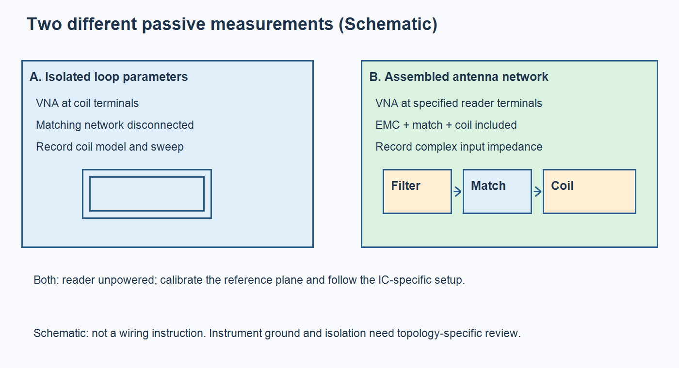
For direct passive measurements, keep the reader unpowered and use the vendor-approved connection and stimulus conditions. Calibrate the cable and fixture to the intended measurement plane. NXP’s guide emphasizes calibration close to the reader transmit terminals. An added adapter or long probe connection should not silently become part of the reported antenna.
Check instrument-ground connections before attaching a differential circuit. A USB, oscilloscope, or supply connection may create an additional path. Follow the documented setup for that IC; do not treat a coaxial shield as permission to ground an arbitrary antenna terminal.
Save the raw sweep and a setup photograph with a simple circuit sketch. A screenshot labeled only “antenna good” cannot establish whether the coil, matching network, or an unintended fixture was measured. If prototype assembly access is unresolved, share the schematic, layout, and measurement-access questions with the planned build quantity so manufacturing access and quotation assumptions can be reviewed before ordering.
Tune in the final mechanical arrangement
The enclosure, nearby metal, ferrite, and antenna cable belong in the tuning configuration. A free-space board measurement is a development baseline; it does not establish the performance of the mounted product.
TI’s TRF79xxA antenna design guide (SLOA241C, revised March 2020) explains that nearby metal can change coil behavior and reduce performance. Where ferrite is used to manage metal proximity, TI calls for measurement and tuning with that ferrite and the final enclosure present. Large PCB copper planes also require attention around the loop.
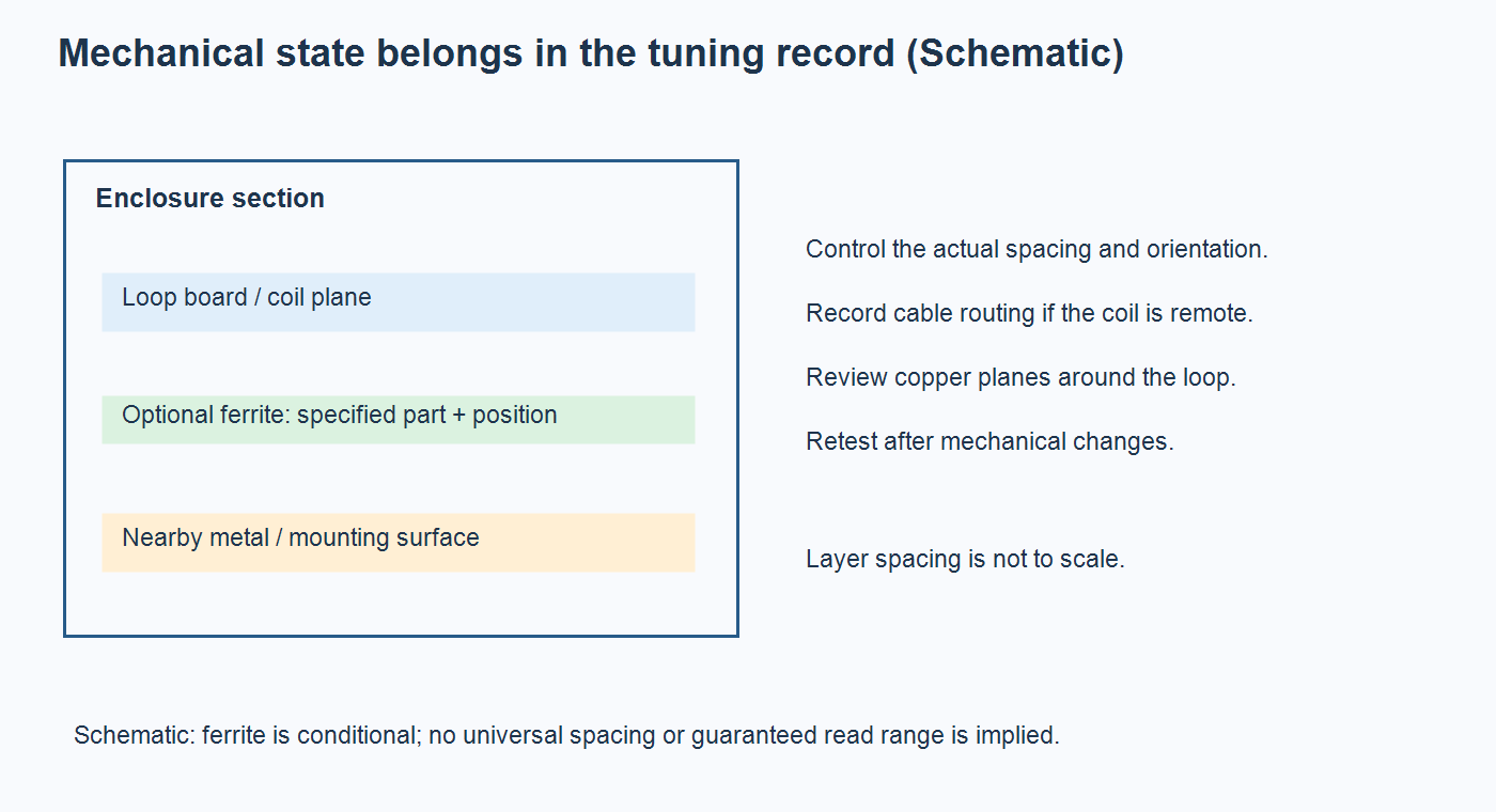
Put the mechanical configuration in the test record: enclosure revision, mounting surface, coil position, ferrite identity and placement, and any remote-antenna cable routing. Define the card presentation direction and intended operating region. Avoid describing performance with an unexplained maximum-distance number.
For example, if an access reader passes on a plastic bench fixture but fails after installation on a metal mounting plate, reproduce that installed state before adjusting the match. Compare the coil and network measurements against the original setup, then repeat powered checks. Buying another capacitor assortment does not resolve an uncontrolled mechanical difference.
Balance bandwidth, field strength, and reception
Select the system response for the required communication modes rather than maximizing coil Q. Quality factor, or Q, describes resonant behavior, but its meaning depends on which circuit and measurement method produced it.
A coil’s unloaded Q and a populated system’s effective Q are different results. TI’s guide discusses bandwidth needed for communication sidebands, particularly at higher data rates. A narrow response that produces a strong carrier can still be unsuitable for the required modulation. Record the method and bandwidth definition whenever Q is reported.
Use the selected manufacturer’s model to explore the tradeoff, then confirm it on hardware. ST’s antenna matching tool takes antenna parameters and target matching inputs and supports circuit simulation. Its calculated component values are starting candidates, not evidence that a different PCB or enclosure will pass.
Separate a weak-field problem from a receiver or waveform problem during debugging. Note whether failure changes with position, orientation, mode, or data rate. Keep the driver configuration and supply condition fixed during each comparison. Changing drive settings, damping, and capacitors together makes a better read result difficult to attribute and reproduce.
Approve matching parts and population explicitly
Control exact matching-component identities and fitted states after tuning. The successful prototype BOM must describe what was actually installed, including parallel trim parts, omitted positions, and temporary tuning links.
For each sensitive capacitor, resistor, or filter inductor, review the manufacturer’s relevant tolerance, electrical ratings, frequency behavior, and package data against the circuit requirements. The BOM alternate approval workflow helps keep a purchasing candidate separate from an authorized replacement. Matching nominal capacitance alone does not document the rest of that comparison.
Preserve the approved build as the comparison baseline while evaluating a substitution. Change one defined item at a time, identify the affected reference designators, and retain both component lists with the resulting measurements. Decide whether the evidence supports only an evaluation lot or the intended production configuration. This keeps a temporary sourcing solution from becoming an unexplained tuning revision on a repeat order.
Use the assembly variant-control guide when the same PCB supports different antennas or fitted networks. A footprint retained for tuning does not authorize production to populate it. Link each assembly configuration to its own measured baseline and applicable firmware settings.
| Proposed change | Evidence to compare | Release decision |
|---|---|---|
| Matching-part alternate | Exact device data and measured network response | Approve the defined part and configuration after relevant verification |
| Enclosure, mounting metal, ferrite, or cable change | Recreated mechanical state and powered operating checks | Retain or revise tuning only with evidence for the changed assembly |
| Coil geometry or copper-layout revision | New coil model and completed network response | Recalculate and verify rather than inherit the previous capacitor list |
Verify the powered reader and release an assembly scope
Release the reader when its measured circuit, mechanical configuration, and powered acceptance results describe the same assembly. Keep functional card checks separate from any claimed standards-conformance assessment.
Define the required card types, operating positions, orientations, communication modes, supply conditions, firmware identity, and pass criteria before the trial. NXP’s design guide distinguishes field-strength, waveform, and load-modulation tests using appropriate reference equipment. Reading one convenient card does not establish all those results. Agree the applicable standard edition and required test procedure with the responsible test owner.
The full-turnkey PCB assembly scope connects fabrication, component sourcing, and assembly planning. Specify any RF fixture, tuning, programming, or test-report requirement separately for project review; a general assembly service description does not establish a dedicated contactless certification capability.
A repeatable RFID reader build preserves the measurement boundary, exact population, installed geometry, and acceptance method together. For a planned OrinewPCB assembly build, provide the fabrication files and controlled assembly package, including BOM, placement data, quantities, antenna configuration, and required test scope, so sourcing, assembly, verification responsibilities, and quotation can be aligned.
Latest Blog
Contact Info
Phone: +86-755-82882936
Email: [email protected]
WhatsApp: +86-13570802455
Wechat: +86-13570802455
Address: 2nd floor,D Bldg.,Electric Link Technology Bldg.,Gongming,Guangming New Dist.,518106 Shenzhen, China