
Reading Wiring Diagrams: From Circuit Intent to PCB-Ready Design
Table of Conent
Table of Conent
Reading wiring diagrams is not just a troubleshooting skill. For an electronics team, it is the first check that a design has a coherent electrical intent before that intent becomes a schematic, PCB layout, bill of materials, and assembled product.
A wiring diagram may be simple enough to show a battery, switch, and load, or complex enough to show power distribution, interlocks, connectors, sensors, and control circuits across several pages. In either case, the useful question is the same: what must connect to what, under which condition, and through which return path? Answering that question accurately helps prevent missing nets, reversed polarity, unsuitable connector pinouts, and late changes after layout begins.
What a Wiring Diagram Tells You
A wiring diagram describes functional electrical relationships. It identifies components, terminals, wires or nets, and the intended paths between them. A diagram is not necessarily a physical layout. The location of a symbol on a page rarely indicates where a component should sit on a PCB or in an enclosure.
Before tracing individual wires, identify four pieces of context:
- Power source and reference: Find the supply rails, voltage labels, protective devices, and ground or return symbols.
- Inputs and outputs: Identify where signals enter, where they are processed, and what they control.
- Control conditions: Look for switches, relays, logic states, enable lines, or interlocks that change the circuit behavior.
- Boundaries: Connectors, terminal blocks, cable labels, and page references often show where responsibility passes between boards, harnesses, and external equipment.
This system-level pass prevents a common error: treating every drawn line as an isolated wire instead of understanding how power, signals, and returns work together.
Recognize Symbols Before You Trace the Circuit
Most wiring diagrams use standardized symbols, but symbol style can vary by CAD library, region, or industry. Read the legend when one is supplied. Without a legend, confirm unfamiliar symbols against the documentation used for that project rather than relying on visual similarity.
Pay particular attention to polarized and direction-sensitive parts:
- Diodes, LEDs, electrolytic capacitors, and batteries have polarity.
- Transistors, MOSFETs, and optocouplers have terminals with distinct functions.
- Relays separate coil contacts from switched contacts, even when the symbols are placed far apart.
- Connectors need both a connector reference and an unambiguous pin number.
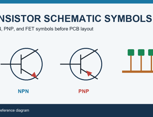
For a more focused reference on device notation, see this guide to transistor schematic symbols. That detail matters because a symbol that looks almost right can still represent the opposite transistor type, an incorrect pin order, or a different control behavior.
Labels are equally important. A net named +12V, CAN_H, ENABLE, or J3-4 can connect points that are not visually adjacent. Treat a repeated net label as an intentional electrical connection only when the drawing convention confirms it. A crossing pair of lines is not automatically a junction; many drawing systems use a dot to distinguish a joined node from a simple crossing.
Read the Diagram as a System
Start with the circuit’s energy path. Follow power from the source through protection, switching, conversion, and the load. Then trace the return path. A circuit may appear complete on the positive side while its ground, chassis, or signal return is missing or routed through an unintended path.
Next, trace the control path. For example, a low-side MOSFET driver may receive a logic signal, pull the load return toward ground, and require a flyback diode if the load is inductive. The diagram should make each of these relationships visible: supply, driver, load, protection, and return.
For multi-page documentation, record every off-page connector and cross-reference as you encounter it. Do not assume a similar label on another page is the same node. Confirm the page number, zone reference, connector designation, and pin number.
Trace a Circuit Methodically
Use one repeatable method for each functional block:
- Pick a source, such as a battery terminal, regulated rail, sensor output, or communication connector.
- Follow the path through each component and net label until it reaches a load, input, or boundary connector.
- Identify the intended return route and any protective or switching component in that route.
- Note values, ratings, pin numbers, and configuration options that change the path.
- Repeat the process in the reverse direction from the load or output back to its source.
This two-way check is useful because it exposes assumptions. A wire that seems to supply a relay coil may actually reach a normally-open contact. A connector label may look correct while the pin numbering is mirrored between the mating views. When working from a harness drawing, verify whether the view is defined from the wire-entry side or the mating face.
Color codes can help during assembly and service, but they are not a substitute for net identity. Production documentation should still define connector pinouts, wire gauges where relevant, net names, and revision-controlled drawings.
Translate the Diagram Into a PCB
A wiring diagram can define the functional intent, but a PCB requires implementation decisions that the diagram alone may not answer. Before layout, resolve the following:
Create a complete netlist
Every intended electrical connection needs a named or otherwise controlled net. Avoid recreating connections manually in PCB software from a visual reference. A linked schematic and PCB flow provides a netlist that can flag unconnected pins, accidental shorts, and changes between revisions.
Check footprint and connector reality
A correct schematic symbol does not prove that the installed part will fit. Confirm package dimensions, pad geometry, connector orientation, keying, pin numbering, and mating clearance against the component datasheet and mechanical design. For wire-to-board connections, specify whether a drawing’s pin sequence is viewed from the board side, cable side, or mating face.
Separate electrical roles in the layout
The diagram may show one common ground symbol, but layout must account for current paths, noise coupling, and reference continuity. Keep high-current or switching loops compact. Place decoupling capacitors close to the relevant power pins. Route sensitive analog or high-speed signals with their return paths in mind instead of treating ground as an unlimited, interchangeable connection.
Make test and assembly needs visible
Include programming pads, test points, fiducials, polarity marks, and assembly notes where the product requires them. These are not decorative additions. They affect test coverage, setup time, rework risk, and the ability to verify that the manufactured board matches the intended circuit.
Before releasing Gerbers, it is useful to evaluate a PCB manufacturer before sending Gerbers so your drawing package and fabrication assumptions can be reviewed together. When the project proceeds to assembly, the relevant service path is PCB assembly service.
Common Diagram-to-PCB Errors
Several failures occur when a correct-looking drawing is handed off without an implementation review:
- Unconnected or mislabeled nets: A net label differs by one character, or a connector pin is omitted from the schematic.
- Reversed polarity or orientation: The symbol is correct, but the footprint pin mapping, diode stripe, IC pin-1 mark, or connector view is wrong.
- Missing protection: A supply path lacks a fuse, reverse-polarity strategy, transient protection, or flyback path required by the load and environment.
- Inadequate current path: Trace widths, copper weight, vias, connector ratings, or return paths do not suit the expected current.
- Assumed substitutions: A component alternate changes package, pinout, tolerance, voltage rating, or operating behavior without a schematic and footprint review.
The handoff package should make these issues discoverable before production. A useful baseline is the Gerber set, BOM with manufacturer part numbers and approved alternates, pick-and-place file, assembly drawing, revision notes, required quantity, and test requirements. The existing guide to a PCB assembly order package explains why those files need to agree with one another.
If your team has a wiring diagram or schematic but is uncertain about connector mapping, footprints, or assembly notes, send the design package for an engineering review. Include the current schematic or wiring diagram, Gerbers if available, BOM, connector details, required quantity, and any test or programming requirements.
A Practical Release Checklist
Before treating a wiring diagram as PCB-ready, confirm that:
- Every power source, load, control input, and return path has been traced.
- All connectors have confirmed pin numbers, views, keying, and mating information.
- Polarized components and direction-sensitive devices have verified symbol-to-footprint mappings.
- Protection, current capacity, voltage ratings, and thermal constraints suit the intended use.
- The schematic, PCB netlist, BOM, assembly drawing, and manufacturing files share the same revision.
- Test, programming, inspection, and special assembly requirements are explicit.
Conclusion
Good electrical diagram reading connects circuit intent to a manufacturable implementation. Read the system before the individual wire, validate symbols and connector views, trace both the power and return paths, and resolve every physical detail that a PCB needs but a conceptual drawing may omit.
When the design package is ready, submit the files for a PCB assembly review. Provide the latest Gerbers, BOM, pick-and-place data, assembly drawing, quantity, and test requirements so the review can focus on the decisions that affect assembly and verification.
References for Technical Verification
- International Electrotechnical Commission, IEC 60617 graphical symbols for diagrams: https://www.iec.ch/homepage
- IPC, standards and guidance for electronics manufacturing: https://www.ipc.org/
Latest Blog



Contact Info
Phone: +86-755-82882936
Email: [email protected]
WhatsApp: +86-13570802455
Wechat: +86-13570802455
Address: 2nd floor,D Bldg.,Electric Link Technology Bldg.,Gongming,Guangming New Dist.,518106 Shenzhen, China