
Open Drain Vs Push Pull: Key Differences and PCB Design Implications
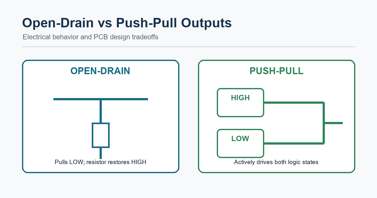
Table of Conent
Table of Conent
An open-drain output can actively pull a signal low but needs a pull-up resistor or another current source to create the high state. A push-pull output uses complementary transistors to drive both high and low. That structural difference affects bus sharing, voltage translation, edge speed, static current, electromagnetic emissions, and fault behavior on a PCB.
The practical choice is not simply "slow versus fast." Open-drain is useful when several devices must share one line or when the high level must be set by a separate voltage domain. Push-pull is usually better when a single driver needs fast, efficient transitions. The correct design comes from the interface requirements and the component datasheets, not the label alone.
Open-Drain and Push-Pull Outputs at a Glance
| Design question | Open-drain output | Push-pull output |
|---|---|---|
| How is LOW driven? | An internal transistor sinks current to ground | The low-side transistor actively drives LOW |
| How is HIGH driven? | An external pull-up or current source restores HIGH | The high-side transistor actively drives HIGH |
| Can multiple outputs share a line? | Yes, when the protocol and device ratings allow wired logic | Generally no; opposing drivers can create contention |
| Edge behavior | Falling edge can be fast; rising edge is RC-limited | Both edges are actively driven and usually faster |
| Static current | Current flows through the pull-up while LOW | Ideally little DC load current in either stable state |
| Voltage translation | Often possible with the pull-up tied to a compatible rail | Usually tied to the driver’s supply domain |
| Typical uses | I2C, SMBus, interrupt lines, reset lines, fault flags | SPI, clocks, chip selects, GPIO control, many point-to-point links |
These are architectural tendencies, not universal specifications. Some pins offer selectable modes, integrated pull-ups, slew-rate control, open-source behavior, or current-limited outputs. Always verify the actual pin type, voltage tolerance, drive strength, leakage, and timing in the device datasheet.
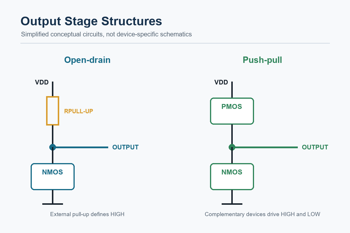
Simplified conceptual output stages. Actual IC implementations vary.
How an Open-Drain Output Works
The output transistor in an open-drain stage acts as a controlled path to ground. When it turns on, the pin sinks current and produces a low level. When it turns off, the pin becomes high impedance. The external pull-up resistor then charges the line capacitance toward its supply voltage.
This arrangement has two important consequences. First, a released line is not the same as an actively driven high. The high state depends on the pull-up network, leakage currents, connected devices, and capacitance. Second, multiple open-drain outputs can connect to one net because each device either pulls low or releases the line. If any device pulls low, the line stays low. That behavior supports shared interrupt nets and wired-AND logic in positive logic.
I2C is the familiar example. Its serial data and serial clock lines use open-drain or open-collector behavior so multiple devices can share the bus, acknowledge transfers, and support arbitration. The bus still needs a valid pull-up design. A line with no pull-up may float, while a resistor that is too large may produce a rise time that violates the timing requirement.
Open-drain is also useful for certain level-translation cases. The pull-up can connect to a rail different from the output device’s core supply, but only if every connected pin is tolerant of that voltage in every power state. A 5 V pull-up connected to a 3.3 V pin is not automatically safe. Check absolute maximum ratings, input clamp behavior, power-off tolerance, leakage, and back-powering conditions.
How a Push-Pull Output Works
A push-pull stage normally uses a high-side transistor and a low-side transistor. The high-side device sources current to drive the output high, while the low-side device sinks current to drive it low. The control circuitry prevents both devices from remaining fully on at the same time during normal operation.
Because both states are actively driven, push-pull outputs can charge and discharge load capacitance much faster than a comparable resistor-pulled open-drain line. They also avoid continuous pull-up current when the signal is low. Those properties make push-pull a common choice for point-to-point clocks, SPI signals, chip selects, enables, and general-purpose outputs.
The main restriction is driver sharing. Two push-pull outputs must not drive the same net unless the device documentation explicitly defines a safe coordination method. If one output drives high while another drives low, the path from the supply rail to ground may be limited mainly by the output transistors and interconnect resistance. The result can be excessive current, logic errors, heating, or damage.
Pull-Up Resistance, Capacitance, and Rise Time
An open-drain line rises approximately as an RC charging waveform. The pull-up resistance and total bus capacitance set the time constant:
tau = Rpull-up x Cbus
For a first-order RC network, the approximate 30% to 70% rise time is:
tr approximately 0.8473 x Rpull-up x Cbus
This equation is useful for an initial design estimate. The total capacitance includes IC pins, PCB traces, connectors, cables, probes, and other attached devices. The final resistor must satisfy two opposite limits:
- It must be low enough to charge the line within the required rise time.
- It must be high enough that every active device can sink the resulting low-state current while maintaining a valid output-low voltage.
For example, a 4.7 kOhm pull-up with 100 pF of total bus capacitance gives an estimated 30% to 70% rise time of about 398 ns. That may suit one interface mode and fail another. Lowering the resistor to 2.2 kOhm shortens the estimate to about 186 ns, but it also more than doubles the current that a device must sink when the line is low.
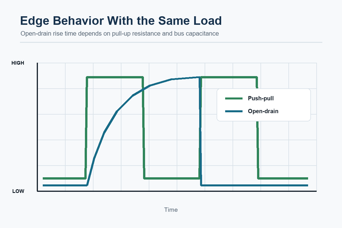
Conceptual edge comparison with the same capacitive load; the diagram is not a measured waveform.
Use the timing limits and calculation method defined by the applicable interface specification. Texas Instruments’ application note on I2C bus pull-up resistor calculation shows how rise-time and output-low constraints bound the resistor range. Datasheet values still control the behavior of the actual parts on the board.
Preparing an interface for fabrication or assembly review? Submit the schematic, Gerbers, BOM, required bus speed, cable or connector details, and any test limits through the assembly quotation page. The package can then be checked for component, layout, and test requirements before quotation.
Signal Integrity, EMI, and Power Tradeoffs
Faster is not always better. A push-pull output with high drive strength can create short rise and fall times that excite trace discontinuities, increase ringing, and raise radiated or conducted emissions. A series resistor placed near the driver may help control the edge and source impedance, but its value should be selected from the driver characteristics, interconnect geometry, receiver thresholds, and measured behavior.
Open-drain edges are asymmetric. The active pull-down can produce a relatively fast falling edge, while the resistor-capacitance network produces a slower rising edge. The slower edge may reduce some high-frequency energy, but excessive rise time reduces noise margin at the sampling instant and leaves the signal longer in the receiver’s transition region. A slow edge can also increase current in some CMOS inputs or create multiple transitions when noise crosses the threshold.
Static power is another tradeoff. An open-drain line dissipates power while low because current flows through the pull-up. The approximate resistor current is (Vpull-up - VOL) / Rpull-up. Push-pull outputs normally avoid that continuous pull-up loss, although they draw transient current while charging capacitance and may experience brief cross-conduction during switching.
PCB Design Implications
Confirm pin behavior before routing
The schematic symbol or firmware name does not prove the electrical output type. Confirm whether each pin is open-drain, push-pull, tri-state, configurable, or input-only. Record the power domain, absolute maximum voltage, input thresholds, output current limits, leakage, and power-off behavior. If you are translating circuit intent into layout, the guide to reading wiring diagrams for PCB-ready design provides a useful handoff framework.
Place pull-ups deliberately
A pull-up is a functional component, not an afterthought. Place it where it supports the required signal path and makes the voltage domain clear. On a short, low-speed board-level bus, the exact physical position may be forgiving. On a longer or faster interconnect, analyze the line topology, stubs, connector capacitance, and termination strategy rather than treating the net as a lumped node.
Avoid scattering undocumented pull-ups across modules. Parallel resistors reduce the effective resistance, increasing low-state current and changing rise time. Include the value and rail in the schematic and BOM so the assembled board matches the electrical calculation.
Control return paths and coupling
Route the signal over a continuous reference plane where practical. Keep return-path discontinuities, long stubs, and unnecessary loops under control. Separate sensitive analog nodes from fast digital edges, and review connectors or cables that add capacitance or expose the signal to external noise. General PCB layout design considerations still apply even when the digital protocol appears slow.
Plan test access
Add accessible test points when validation or production testing needs to observe the line. A probe adds capacitance, so specify an appropriate measurement method for a rise-time check. Test both stable voltage levels and transitions. For shared open-drain nets, verify that each participant can assert and release the line independently.
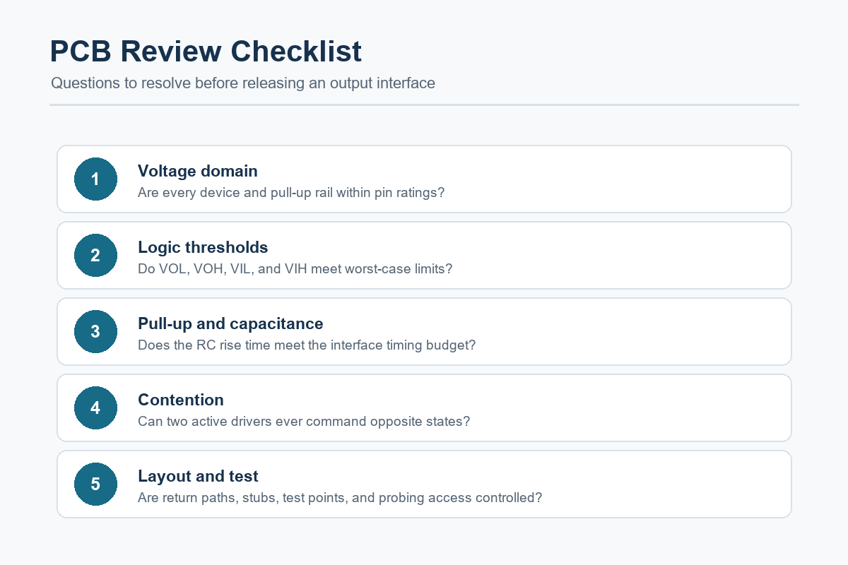
Five checks to complete before releasing an output interface to PCB production.
Common Design Errors
Missing or incorrect pull-up
An open-drain output without a pull-up has no defined high-state source. An internal pull-up may be too weak or too variable for the required timing. Conversely, a pull-up that is too strong may exceed the output’s sink-current or low-voltage specification.
Connecting incompatible voltage domains
The pull-up voltage must be safe for every connected device, including when one device is powered down. Check clamp-diode current and back-powering risks instead of relying only on nominal logic levels.
Tying push-pull outputs together
Shared-line behavior that works with open-drain outputs does not transfer to push-pull GPIO. If several devices need to signal one controller, use open-drain outputs, a logic gate, a multiplexer, or another defined interface architecture.
Ignoring default and startup states
Many pins start as inputs and change mode after reset. Pull-ups, pull-downs, boot straps, and peripheral configuration can create a temporary state that differs from normal operation. The article on computer jumpers and PCB configuration illustrates why hardware configuration states need explicit documentation.
Substituting parts without checking the output stage
Two devices with similar functions may use different output structures, drive strengths, voltage tolerances, or default modes. A BOM substitution can therefore change edge rate, current, or bus compatibility even when the package and basic pinout match.
A Practical Selection Framework
Choose open-drain when the design needs one or more of these behaviors:
- Multiple devices must safely assert the same line.
- The protocol requires wired logic, acknowledgment, or arbitration.
- A compatible external pull-up rail provides intentional level translation.
- A default released state must remain defined while devices reset or disconnect.
Choose push-pull when the design instead needs:
- A single, coordinated driver on the net.
- Fast and controlled transitions in both directions.
- Lower static loss than a resistor-pulled line that spends substantial time low.
- Direct point-to-point control without wired logic.
Some designs need both. A microcontroller may use open-drain pins for I2C and fault signals while using push-pull outputs for SPI clocks, chip selects, and control lines. The PCB assembly service overview can support the manufacturing handoff after those electrical decisions are documented in the schematic, BOM, layout, and test requirements.
Release Checklist
Before releasing the board, confirm the following:
- Every output pin’s electrical mode and startup state are documented.
- High- and low-level thresholds meet worst-case datasheet limits.
- The open-drain pull-up satisfies both rise-time and sink-current constraints.
- Total capacitance includes traces, connectors, cables, pins, and test fixtures.
- No push-pull outputs can contend during startup, normal operation, or faults.
- Pull-up rails remain safe during partial-power and power-off conditions.
- Fast push-pull edges have been reviewed for ringing, crosstalk, and EMI.
- Test points and acceptance limits are included where production verification requires them.
Conclusion
Open-drain outputs trade active high-side drive for safe line sharing and flexible pull-up behavior. Push-pull outputs actively control both states, providing faster edges and lower static loss for point-to-point signals. Neither architecture is inherently superior. The correct choice follows from bus ownership, voltage domains, timing, capacitance, current, startup behavior, and PCB interconnect conditions.
For a manufacturing review and quotation, send the latest Gerbers, BOM with manufacturer part numbers, pick-and-place data, assembly drawing, required quantity, and interface test requirements through the free quote page. The submitted package can then be reviewed for fabrication, assembly, component, and test requirements before pricing.
Latest Blog


Contact Info
Phone: +86-755-82882936
Email: [email protected]
WhatsApp: +86-13570802455
Wechat: +86-13570802455
Address: 2nd floor,D Bldg.,Electric Link Technology Bldg.,Gongming,Guangming New Dist.,518106 Shenzhen, China