
EasyEDA PCB Design: A Beginner’s Manufacturing Checklist
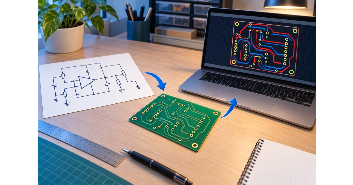
Table of Conent
Table of Conent
EasyEDA can help a beginner move from a circuit idea to a PCB layout, but a routed design is only one part of a successful build. The manufacturer also needs clear fabrication requirements, consistent production files, and enough information to resolve questions without guessing. If assembly is included, component identity and placement data become equally important.
This guide follows that handoff from schematic review to a fabrication-ready package. It focuses on engineering checks that remain useful even when the editor interface changes. The goal is a first board that can be reviewed, quoted, manufactured, and assembled against a controlled revision.
Identify the editor edition before following a tutorial
EasyEDA Standard and EasyEDA Pro have separate documentation and interface workflows. Start with the guide for the edition you actually use. The EasyEDA Standard introduction describes schematic capture, PCB layout, design-rule checking, and manufacturing exports. The EasyEDA Pro quick-start guide separately documents exports for Gerber fabrication data, the bill of materials, and pick-and-place coordinates.
Do not combine menu instructions from different editions or assume an old tutorial describes the current export dialog. Record the editor edition with your release notes and preserve the native project alongside the manufacturing package. A production team should be able to identify which revision produced the files it receives.
Review the circuit before converting it to a board
Check component values, power connections, connector pin assignments, and signal names against the intended circuit. Investigate warnings rather than dismissing them simply to reach a clean report. Where a warning is intentional, document why it is acceptable so a later reviewer can understand the decision.
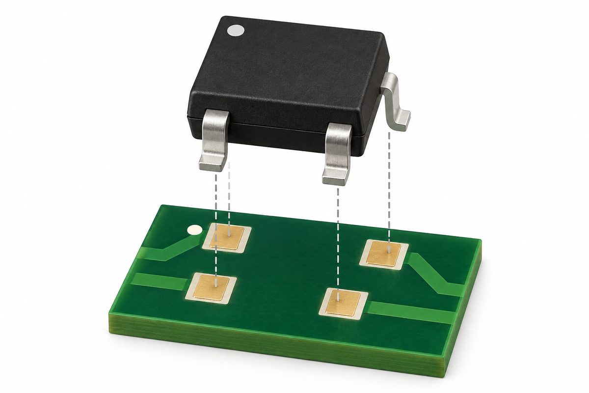
Separate the electrical symbol from the physical footprint. A symbol can describe the correct function while linking to the wrong package or pin numbering. For each critical part, compare the selected footprint with the manufacturer drawing: package dimensions, pad arrangement, pin-one orientation, mounting features, and any exposed pad.
Pay particular attention to connectors and polarized devices. A reversed pin assignment or a footprint viewed from the wrong side can survive basic routing checks and still make the assembled board unusable. Review the mating connector and cable orientation as part of the circuit, not as a separate detail to address after fabrication.
Set the mechanical boundaries and manufacturing rules
Define the board outline, mounting holes, connector positions, and keepouts before detailed routing. Check the board against the enclosure and the neighboring assemblies. If a connector protrudes past the outline, confirm that its position and assembly clearance are deliberate.
Set routing and spacing rules using the proposed fabrication process. A rule checker can only evaluate the constraints you supply; it cannot infer every requirement of an enclosure, high-current path, or sensitive analog circuit. Ask the fabricator about features that need special review before assuming that a small minimum dimension is suitable for the whole design.
For multilayer work, identify layer functions and reference planes early. Overall layer count alone does not define the dielectric spacing or controlled-impedance construction. The multilayer PCB design and production guide explains the broader release considerations that should accompany the editor project.
Place components with assembly in mind
Give the assembler space to place, inspect, and handle the parts. Check whether tall components obstruct nearby pads or whether connectors make soldering and inspection difficult. Keep polarity and orientation markings readable where practical, and ensure reference designators do not obscure pads or important features.
For a prototype, consider access for measurement, programming, and debugging. A board that powers up but offers no practical access to the required signals can slow validation. Identify the test and programming connections before routing makes them hard to reach.
Review both sides of the board and the assembly sequence. Components that are easy to place individually may create a conflict when the board is soldered, depanelized, or installed. Discuss unusual mechanical parts, wires, and secondary operations in the quote request rather than assuming they are covered by a standard assembly step.
Complete routing and examine the result
Resolve unrouted connections and review the design-rule report. Check copper clearances near the outline, holes, and connector regions. Verify the intended connectivity after changes to copper areas, component placement, or net assignments. A final visual pass should complement the automated checks.
If the fabrication plan depends on a specific stackup, reconcile that construction with your layout assumptions. Copper distribution and dielectric construction affect the manufacturing review, particularly on a dense multilayer board. The PCB lamination and process-control guide explains why those inputs should be reviewed together.
Do not treat a clean design-rule report as proof of circuit functionality, thermal performance, or complete manufacturability. It is evidence that the checked geometry meets the configured rules. Other product requirements still need the appropriate analysis and prototype validation.
Export fabrication data and inspect the exported files
Use the export workflow documented for your editor edition. The EasyEDA Standard manufacturing workflow identifies Gerber generation and distinguishes fabrication data from BOM and placement information needed for assembly. Confirm the contents of the actual package you export instead of relying on the name of a ZIP archive.
Inspect the exported layer and drill data in a suitable viewer. Check the outline, layer order, solder-mask openings, silkscreen, and the alignment of drilled features. Make sure the fabrication requirements explain plated and nonplated holes, slots, and any special routing feature clearly enough for the supplier to review.
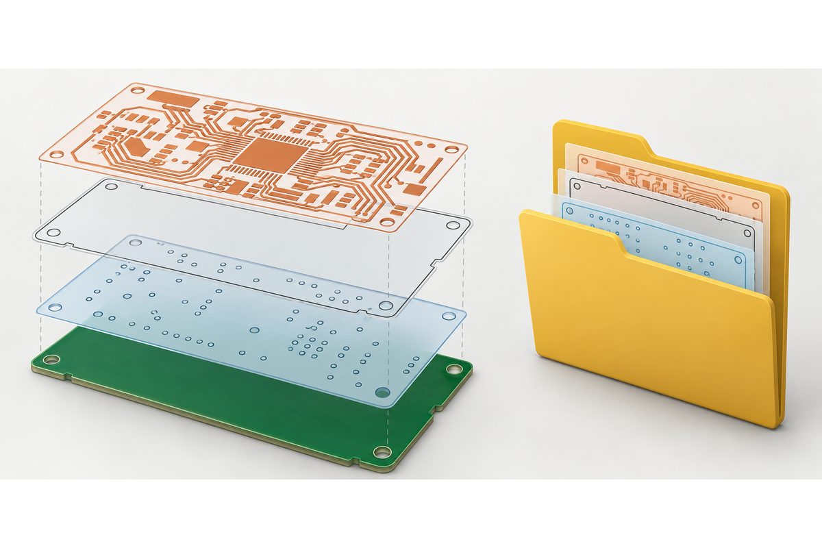
Compare the export with the intended board dimensions and the released project. Look for missing layers, unexpected objects, or outdated revision markings. A native project that looks correct does not guarantee that the exported manufacturing package contains the same intended information.
Before the first fabrication order, submit the Gerber package, drill data, fabrication drawing, stackup requirements, quantity, and schedule through the PCB engineering and quotation request. State any unresolved questions so the engineering review can address them before the production assumptions are finalized.
Add a complete assembly package when parts are required
A fabrication archive alone does not describe what components to purchase or where to place them. Provide a BOM with reference designators, quantities, manufacturer part numbers, and the information needed to distinguish package variants. Identify parts that must not be fitted and state which substitutions require approval.
Supply placement coordinates and an assembly drawing with consistent reference designators. Confirm the coordinate origin, units, board side, and rotation convention with the assembler. For a part with ambiguous orientation, the component drawing and assembly view should provide enough evidence to resolve the question.
Do not assume a supplier-specific library identifier is a complete purchasing specification for another assembler. Give the manufacturer identity and approved part number where procurement is included. If you supply components yourself, identify the quantities, packaging, and any handling requirement the assembly team needs.
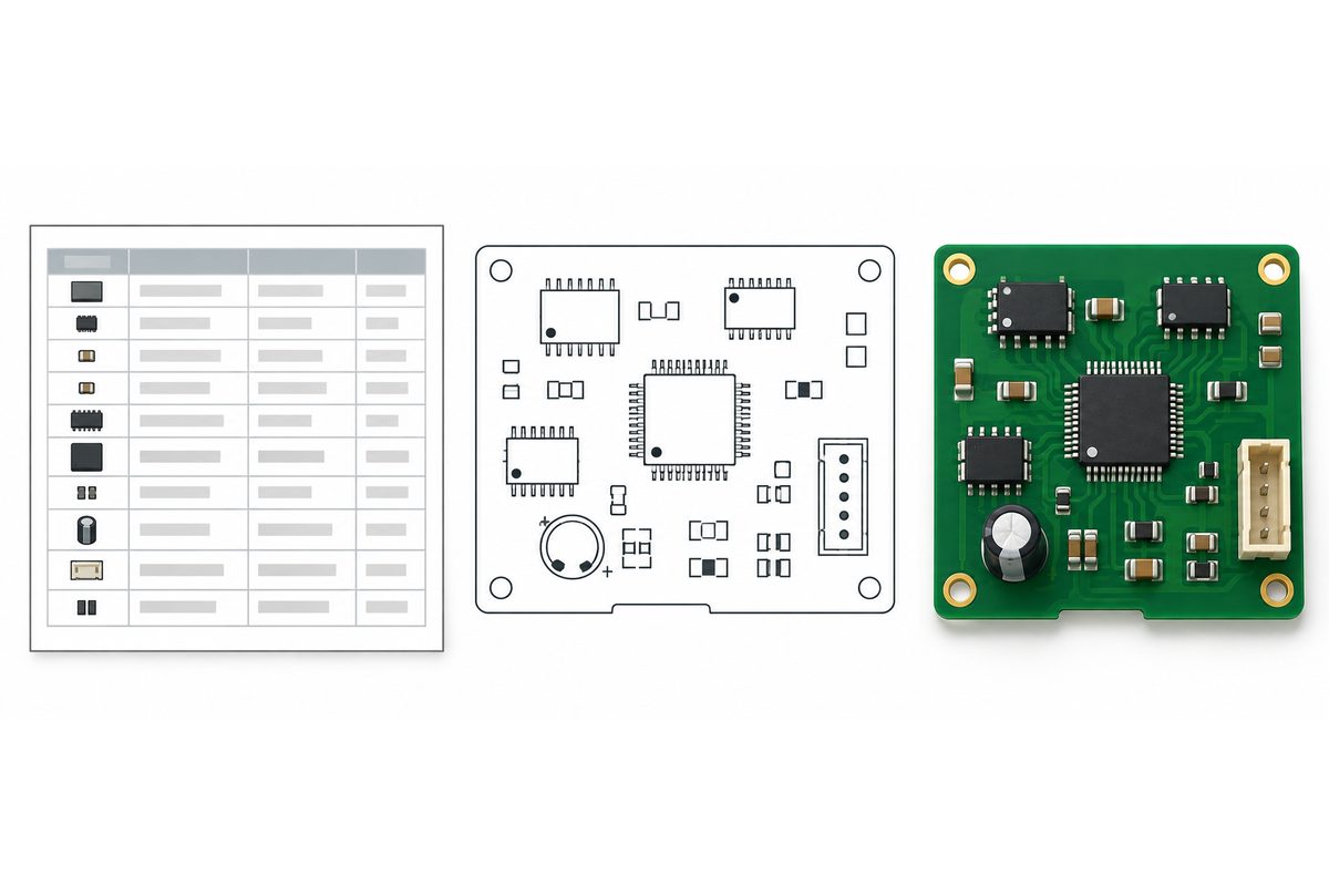
Review the PCB manufacturing capabilities against the fabrication requirements before requesting a combined build. For assembly scope, include the BOM, placement data, assembly drawing, quantity, sourcing preferences, and test expectations in the project quote request so the team can assess the required work and quotation inputs.
Release one consistent revision
Keep the schematic, layout, fabrication files, BOM, and placement data synchronized. A last-minute component change may require a new footprint, updated routing, revised purchasing data, and another export. Sending a new BOM beside an old fabrication archive creates a mismatch even if each file is individually valid.
Use a clearly identified release package and retain the native project that generated it. Include a short description of changes since the previous build and identify any approved exceptions. When the supplier asks a question, record the resolution against that revision rather than leaving it in an unrelated conversation.
For prototypes, plan how you will evaluate fit, power-up, programming, and the important circuit functions. Preserve the observed results and the matching design revision. If the next release changes an interface or critical component, revisit the relevant validation instead of assuming the earlier result still applies.
Conclusion
When comparing quotations, separate bare-board fabrication, component procurement, assembly, programming, and test work. Ask which activities and one-time preparation costs are included. A low quoted board price does not describe the complete assembly scope. Use the same revision, quantity, material assumptions, and test requirements for each comparison, and identify any open questions that could change the estimate. This makes supplier responses easier to evaluate and prevents a prototype order from depending on an unstated purchasing or inspection assumption.
A useful EasyEDA workflow ends with more than a completed layout. Verified footprints, realistic rules, inspected exports, consistent assembly data, and clear release requirements make the first manufacturing handoff easier to review. Those habits also create a better basis for learning from the prototype and preparing the next revision.
Ready to build? Send the released fabrication data, BOM and placement files when assembly is needed, quantity, and testing requirements through the online PCB RFQ form for an engineering and quotation review. Identify the editor edition and unresolved design questions so the review can focus on the actual project.
Latest Blog

Contact Info
Phone: +86-755-82882936
Email: [email protected]
WhatsApp: +86-13570802455
Wechat: +86-13570802455
Address: 2nd floor,D Bldg.,Electric Link Technology Bldg.,Gongming,Guangming New Dist.,518106 Shenzhen, China