
Selective Soldering for PCBs: Joint Maps, Access, and Verification
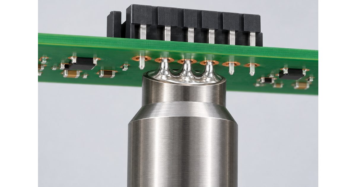
Table of Conent
Table of Conent
Selective soldering applies solder to designated locations instead of exposing the whole board underside to a conventional solder wave. For mixed-technology assemblies, a localized mini-wave process can join through-hole components while working around already assembled surface-mount parts. The process still needs suitable access, materials, thermal conditions, and acceptance evidence.
The useful manufacturing question is not simply whether a board contains through-hole pins. It is whether the intended joints can be reached and soldered repeatably without compromising neighboring features. This guide focuses on the local mini-wave process and the information engineers and buyers should release before a prototype or production order.
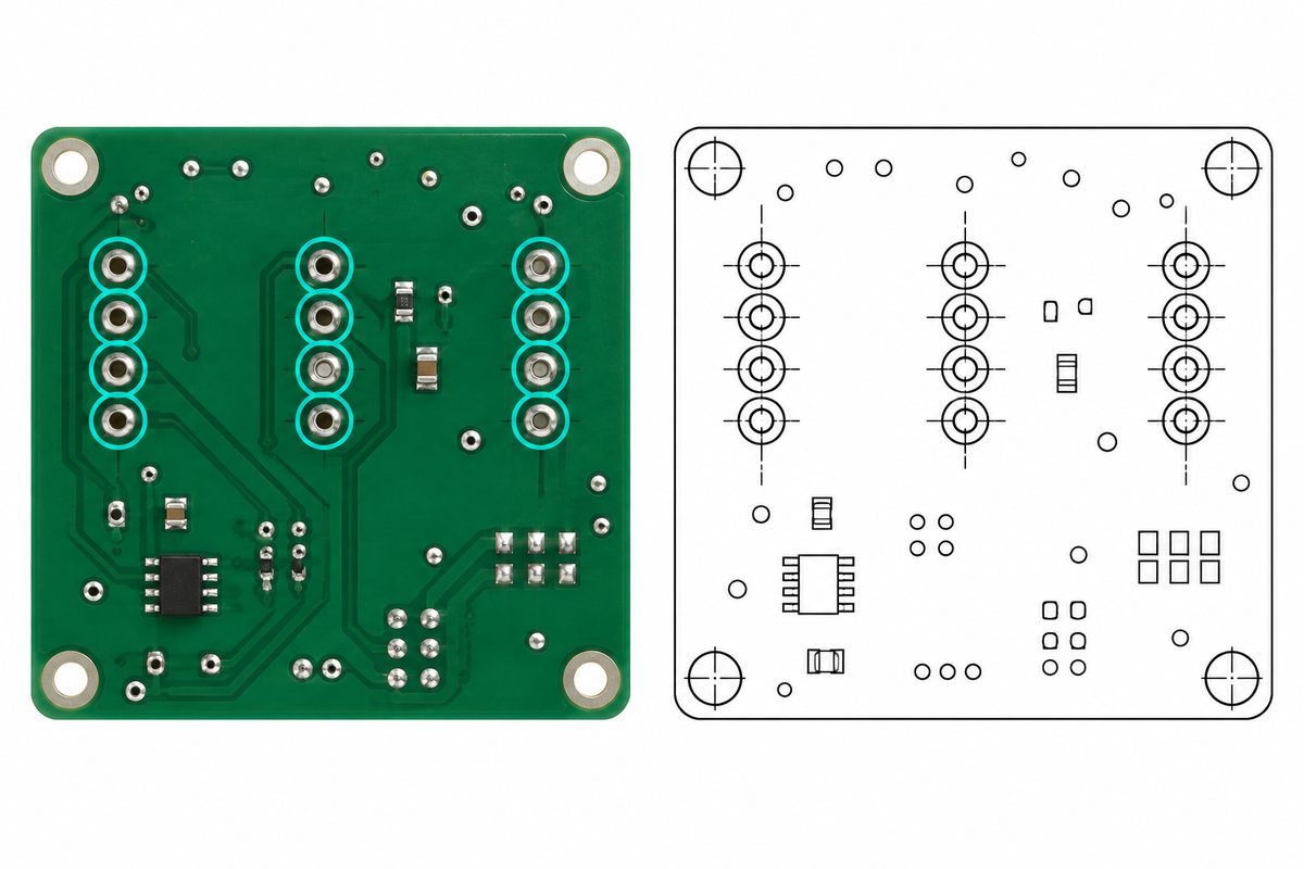
Decide which joints belong in the selective operation
Create a joint map that identifies the component references and pins to be soldered. Distinguish these locations from joints completed by reflow, another soldering operation, or an approved manual step. A bottom-side image without a defined component and pin reference can be difficult to reconcile with the BOM and assembly drawing.
Nordson’s selective soldering overview describes targeting specific board regions around surface-mount packages and controlling local process conditions. This is an equipment-level explanation, not evidence that any particular assembler owns that system or has qualified your board.
Compare the proposed operation with the actual assembly sequence and quantity. Conventional wave soldering, selective soldering, and manual soldering have different access, preparation, and process-control considerations. Select the approach by the joint requirements and verified supplier proposal rather than assuming automation is always the best choice.
Review the underside as a three-dimensional access problem
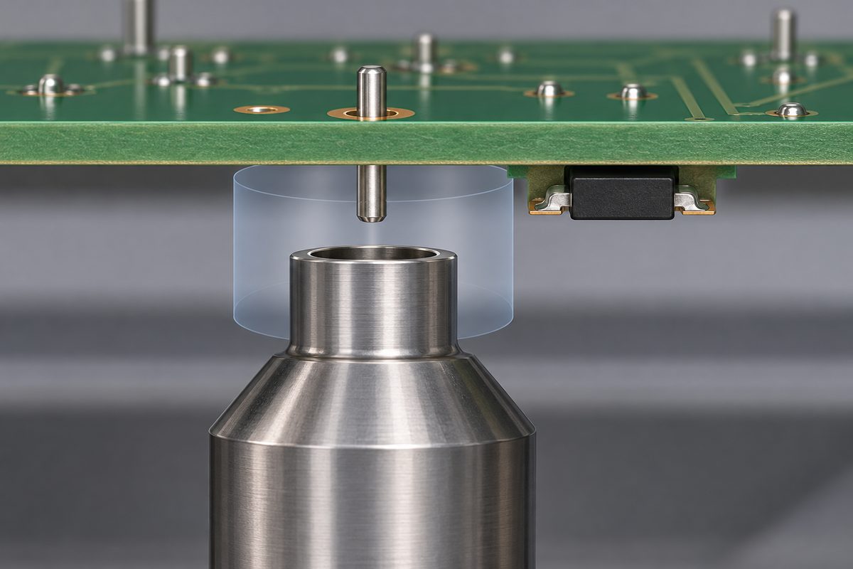
The solder nozzle needs room to reach the intended lands and follow the required approach and departure path. Check the board underside, component bodies, protruding leads, fixtures, and support features. Clearance at the center of a joint does not establish clearance throughout the operation.
Use the proposed nozzle and process envelope in the review. A drawing that shows only the plated-hole diameter misses the space occupied by the tool and local solder wave. Ask the process engineer to identify the relevant equipment-dependent constraints before finalizing nearby component placement.
Review groups of closely spaced pins as well as individual joints. Some features may be suitable for a grouped operation, while others need a different path or tool choice. Keep those decisions in the approved process plan instead of leaving them to a programmer who has not seen the product’s mechanical requirements.
Coordinate lead projection, hole construction, and assembly fit
Define the through-hole component installation and lead projection using the controlled component and assembly requirements. Verify the fit between the lead and finished hole. Do not substitute a drill-tool dimension for a finished plated-hole requirement or assume that a nominal component pin dimension describes its full tolerance range.
Lead projection influences the available access and the geometry encountered by the local wave. Resolve interference with supports, tooling, and neighboring features before programming. A fit that is acceptable during component insertion may still leave a soldering-access issue below the board.
The PCB assembly process guide gives the broader production context. For selective soldering, add a clear handoff between insertion, support, and soldering so the component position assumed by the program matches the actual assembly.
Specify the flux and its intended application area
Identify the flux product and the required material compatibility. The application plan should reach the joints that need flux without treating every nearby surface as a target. Coordinate the delivery pattern with the soldering map rather than assuming the two programs will align automatically.
Review residue and cleaning requirements in the context of the finished assembly. A material designation alone does not answer whether residues are acceptable under the product’s environmental or electrical requirements. If cleaning is part of the plan, confirm access and compatibility with the components and other materials.
Define what happens when the flux application is missing, displaced, or otherwise outside the approved condition. A production recovery should follow a controlled instruction. Adding another pass without reviewing the cumulative exposure is not a substitute for understanding the original condition.
Develop preheat and solder contact as one process
Ersa’s selective soldering process overview separates fluxing, preheating, and mini-wave soldering. It also describes local parameter control. The practical lesson is to coordinate these stages on the actual assembly instead of treating the solder contact as an isolated event.
Review thermal requirements and limits for the board, components, and flux. Thick sections, connected copper, and differently sized terminations can change the local heat demand. Establish the relevant process evidence with the assembler rather than copying one temperature or dwell setting from an unrelated board.
Keep selective-process validation distinct from reflow validation. The reflow soldering guide concerns another thermal operation. A mixed-technology board may experience both, so the manufacturing review must account for the planned sequence and the condition of the assembly entering each stage.
Preparing a mixed-technology prototype? Submit the PCB files, BOM, assembly drawing, target-joint map, quantity, and inspection requirements through the PCB assembly engineering and quotation request. Ask for review of soldering access, materials, and the proposed process sequence before the order scope is finalized.
Turn the joint map into a controlled program
Confirm the board orientation, coordinate reference, and locating method used by the program. The machine must locate the actual joint, not merely the right position on an imported picture. Review the relevant datums and any support or transport arrangement that affects how the board is presented.
Define the selected tool, operation order, approach and departure paths, and approved local process settings. Identify which parameters vary by joint or group and which remain common to the operation. Keep the program revision tied to the released board and assembly revisions.
Before exposing an assembly to solder, use the equipment’s approved setup and clearance-check procedure. Confirm that programmed movement and tooling are compatible with the board. A program that imports successfully is not yet evidence that the machine can execute it safely or that the resulting joints meet the specification.
Validate the result, not only the completion of a cycle
Inspect the intended joints against the applicable acceptance requirements. Depending on the product, the review may address wetting, solder distribution, hole-fill requirements, unintended solder connections, and the condition of adjacent features. Agree on the interpretation, methods, and sample coverage before building the prototypes.
Electrical testing addresses the connections or functions included in its coverage. It does not establish every physical joint characteristic. Similarly, a recorded machine cycle does not prove that flux reached the correct location or that each solder joint met the product requirement.
If special evaluation is required for hidden features or thermal concerns, define it explicitly. Name the sample locations and reporting scope so an evaluation of one convenient joint is not treated as proof of every distinct geometry. Allocate samples deliberately when a method affects the assembly.

Investigate an out-of-condition joint before adjusting the recipe
Record the observed condition, affected component and pin, board revision, material identities, and relevant process settings. Preserve representative evidence before rework. Separate the observation from a proposed cause so the team does not immediately change the wrong variable.
Review access, component fit, flux delivery, and thermal evidence as appropriate to the issue. Change variables in a controlled way during development. Simultaneously changing nozzle, flux, dwell, and joint geometry makes it difficult to identify which change helped or introduced a new problem.
Agree on permitted rework and the required checks afterward. Do not assume that repeatedly running a finished board through the same operation is an acceptable recovery. The product and material limits still apply even when an additional cycle appears convenient.
Release a quotation package with explicit responsibilities
Provide the PCB manufacturing data, BOM, assembly drawing, component documentation where needed, joint map, quantity, and test requirements. Include important underside-access information and identify any proposed fixture or support arrangement. State which process details remain open for engineering review.
Ask how the proposed build fits the through-hole PCB assembly service, with project-specific confirmation for selective soldering. A general service page does not establish that a selected nozzle, flux, board, and local process have been qualified together.
Where programming, tooling, or inspection scope remains unresolved, include those questions in the selective-soldering assembly quotation request. Attach the current files so the review can distinguish one-time preparation from recurring production work and confirm the proposed responsibilities.
Revalidate changes that affect access or the joint
As a hypothetical example, moving an underside component can leave the electrical netlist unchanged while obstructing a previously approved nozzle path. A drawing update therefore needs more than a check that the selected pins still exist. Review the tool envelope and program before repeating the order.
Use the same change-control approach for component substitutions, board construction changes, lead projection, materials, and fixture revisions. Preserve the approved combination and its validation evidence so repeat production follows a known process instead of reconstructing a successful prototype from memory.
Conclusion
Selective soldering succeeds through a coordinated joint map, accessible geometry, compatible materials, controlled thermal process, and verified results. Define these requirements before programming and compare quotations against the same scope. Localized solder application does not remove the need for complete assembly documentation.
Ready to review the build? Send the released PCB files, BOM, marked target joints, quantity, schedule, and inspection requirements through the online PCB RFQ form for engineering and quotation review. Highlight underside-clearance concerns and open process questions so they can be evaluated before production begins.
Latest Blog
Contact Info
Phone: +86-755-82882936
Email: [email protected]
WhatsApp: +86-13570802455
Wechat: +86-13570802455
Address: 2nd floor,D Bldg.,Electric Link Technology Bldg.,Gongming,Guangming New Dist.,518106 Shenzhen, China