
PCB Annular Rings: Drill Allowance, Registration, and DFM Review

Table of Conent
Table of Conent
A PCB annular ring is the copper land surrounding a hole. It provides connection area at a via or plated-through-hole location, but its nominal width in CAD is not necessarily the narrowest width that remains after manufacturing. Hole size, drill position, layer registration, and copper dimensions all influence the finished geometry.
The useful design question is therefore not simply, “Does this pad look large enough?” It is, “Does this pad stack leave the required copper around the applicable hole boundary on every relevant layer, with the agreed manufacturing allowances?” Answering that question before release helps prevent a late pad redesign from disrupting routing or connector fit.
This guide explains the geometry, the documentation needed for a meaningful fabrication review, and how to distinguish design rules from acceptance evidence. It does not prescribe a universal minimum ring or assume that a particular manufacturing process is available for every order.
Start with the correct hole boundary
For a concentric circular pad and circular hole, a nominal radial width can be calculated as:
Nominal ring width = (pad diameter − applicable hole diameter) / 2.
The subtraction gives the total difference across the diameter; dividing by two gives the copper width on one side. The important qualification is “applicable.” A finished plated hole and the production drill tool are not interchangeable dimensions. Copper deposited on the hole wall changes the opening, so a drill selected for a plated hole can be larger than the specified finished opening.
Eurocircuits’ inner annular ring explanation calculates the inner-layer ring from the copper pad and production tool size. Its drill allowance is an example of that supplier’s process, not an AssyPCB parameter or a value to copy into every design. Ask your fabricator which hole boundary its design review uses and how the finished-hole requirement translates into a production tool.

Keep finished-hole size and tolerance in the fabrication package when they control component fit. Do not replace them with an assumed tool diameter without agreement. Conversely, do not treat a nominal ring calculated around the finished opening as proof of adequate inner-layer copper around the drilled opening.
A worked example that is not a design limit
Consider a hypothetical circular land with a diameter of 0.80 mm and an applicable hole boundary of 0.40 mm. With both circles perfectly concentric, the nominal ring is (0.80 − 0.40) / 2 = 0.20 mm. These are example dimensions, not approved minimums or a recommended connector footprint.
Now keep both diameters unchanged and move the hole center 0.05 mm to one side. In this simplified geometry, the narrowest ring becomes 0.20 − 0.05 = 0.15 mm. The opposite side becomes wider. An average or nominal width would conceal the location that has lost margin.
This illustration deliberately ignores diameter variation, etching effects, and other process contributions. A production assessment must address the actual pad and hole dimensions, applicable registration allowances, and the specified acceptance requirement. Do not add unrelated maximum tolerances together without understanding the supplier’s tolerance model; some quantities may already be included in a stated capability.
If a supplier reports a ring value, ask whether it is nominal, minimum after the agreed allowances, or measured on a specific sample. Recording that distinction prevents a CAD value from being mistaken for a finished-board measurement.
Registration makes the narrowest location important
The ring is vulnerable where the hole approaches the land perimeter. On a multilayer board, the same drilled hole passes through lands on different layers, and their alignment matters. An outer view alone cannot demonstrate that every internal connection has the intended geometry.
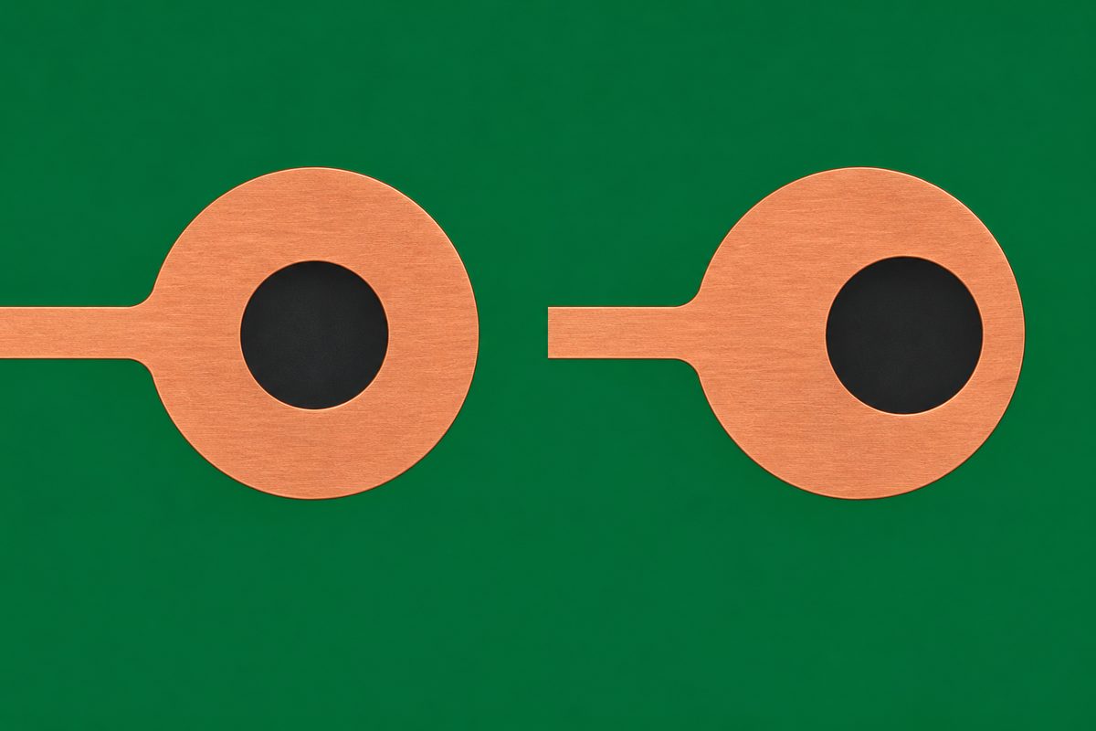
Separate hole location relative to the board from hole-to-land registration. A connector hole can be in an acceptable mechanical position while a particular copper layer has less annular margin than expected. The investigation needs the relevant coordinate relationship, not simply the statement that the drill hit its nominal location.
Also distinguish a visibly narrow ring from breakout, where the hole reaches or crosses the land boundary. Whether a particular condition is acceptable depends on the invoked requirements, connection geometry, product class, and agreed specification. A general web diagram cannot approve a specific board. Record the governing document and revision rather than relying on an unqualified “IPC compliant” note.
Check the pad stack, not only the top layer
A pad stack defines geometry across layers. Review connected lands, any layer-specific pad sizes, hole definitions, and plane clearances together. A top-layer footprint preview may hide an undersized internal land or a configuration that differs from the library’s intended default.
In CAD, apply a scoped annular-ring rule to the appropriate pad and via objects. Altium’s manufacturing rule documentation describes a radial minimum-annular-ring check and its use in online and batch DRC. The rule can flag layout geometry, but its configured limit must reflect the agreed fabrication requirements rather than software defaults.
After changing a pad stack, rerun the relevant checks and inspect the exported fabrication data. Compare a representative connected inner land, an outer land, and any exception footprint. Verify that units, hole attributes, and layer mapping survived export. Keep the released files together so the fabricator does not combine an updated drill file with older copper artwork.
Special via structures need their own review. Our via-in-pad design guide discusses a related application where hole placement and assembly-facing pad requirements must be considered together. A conventional through-hole rule should not automatically be applied to every via construction.
Resolve violations without breaking another requirement
Increasing the copper land may restore annular margin, but it can reduce spacing to nearby traces or adjacent pads. Review electrical clearance, routing channels, plane isolation, and solder mask geometry after the change. A larger land is not a complete fix if it creates a different manufacturing or assembly conflict.
Reducing the hole is another possible geometric change, but it may prevent a connector lead from fitting or violate the component’s specified mounting conditions. Never shrink a connector hole solely to clear a DRC warning. Obtain the relevant component drawing and preserve the intended finished-hole tolerance.
When a dense region cannot accommodate the agreed land and hole combination, identify the affected features and discuss the available alternatives before release. A revised escape layout, different interconnect strategy, or changed component footprint may be more appropriate than relaxing a rule globally.
Use the PCB manufacturing capabilities page as a starting point for the conversation, then confirm the combination required by your actual stackup and hole construction. A general capability listing does not approve an individual pad stack.
If a dense layout has competing fit and clearance constraints, send the copper files, drill data, stackup, and component hole requirements for a fabrication review. Include the affected reference designators and proposed alternatives so the discussion can focus on a specific decision.
Separate copper geometry from solder mask and electrical test
An annular ring is a copper feature. A solder mask opening exposes or covers copper; making that opening larger does not add copper to a land. Inspect the copper and mask layers independently, especially when the visible exposed area makes a pad appear larger or smaller than its underlying land.
Likewise, electrical continuity is not a dimensional measurement of every ring. A board can retain a connection at a narrow location, so a passing electrical test should not be treated as evidence that all specified annular dimensions have been inspected. Use electrical and dimensional evidence for their respective purposes.
For internal features, agree on suitable evidence and sampling. IPC’s IPC-TM-650 2.2.5 dimensional inspection method includes annular ring width and layer-to-layer registration among attributes measurable using prepared microsections. It describes measurement practice, not a universal product acceptance value.
Our PCB microsection analysis guide explains how sample identification and inspection context support interpretation. A selected section documents the feature and location examined; it should not be presented as a measurement of every hole in an entire shipment.
Check the exported release package
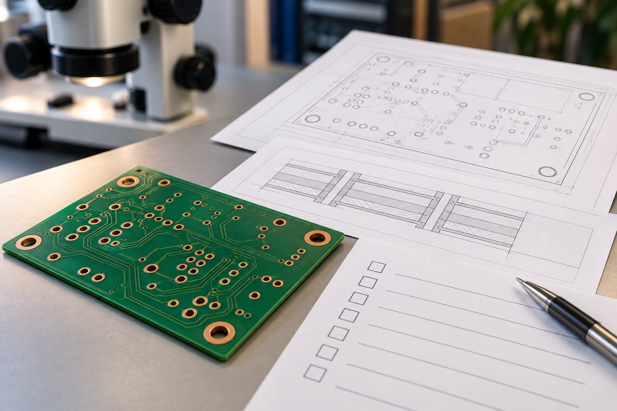
Before placing the order, prepare a concise release checklist:
- Identify plated and non-plated holes and any special via constructions.
- State finished-hole requirements, tolerances, and the governing fabrication specification.
- Check land sizes on relevant layers and identify intentional exceptions.
- Resolve the supplier’s hole-size basis and allowance assumptions.
- Rerun clearance checks after pad or hole changes.
- Match copper, drill, stackup, and drawing revisions in one release package.
- Agree on any dimensional inspection evidence and how it will be identified.
Where a review remains open, request a quote with the unresolved pad-stack locations and required hole tolerances. Ask for clarification before approving a manufacturing change; do not assume that a quotation silently resolves every geometry exception.
Close the loop after a ring-related finding
If inspection reveals an unexpected narrow ring, preserve the board revision, sample identity, layer, hole location, image scale, and measurement basis. Compare that evidence with the released land and drill data. Decide whether the issue comes from the design margin, a mismatched file revision, a misunderstood hole basis, or a manufacturing variation that requires investigation.
Change only the relevant design or process assumption, then verify that the corrective action addresses the observed condition. If you are preparing the next revision, share the affected feature, revised fabrication package, and requested inspection evidence so the next build can be reviewed against an explicit requirement. Reliable annular-ring decisions come from aligned geometry, agreed tolerances, and traceable evidence—not from a single attractive CAD screenshot.
Latest Blog



Contact Info
Phone: +86-755-82882936
Email: [email protected]
WhatsApp: +86-13570802455
Wechat: +86-13570802455
Address: 2nd floor,D Bldg.,Electric Link Technology Bldg.,Gongming,Guangming New Dist.,518106 Shenzhen, China