
ENIG, ENEPIG or Immersion Silver: Specify the Joining Interface
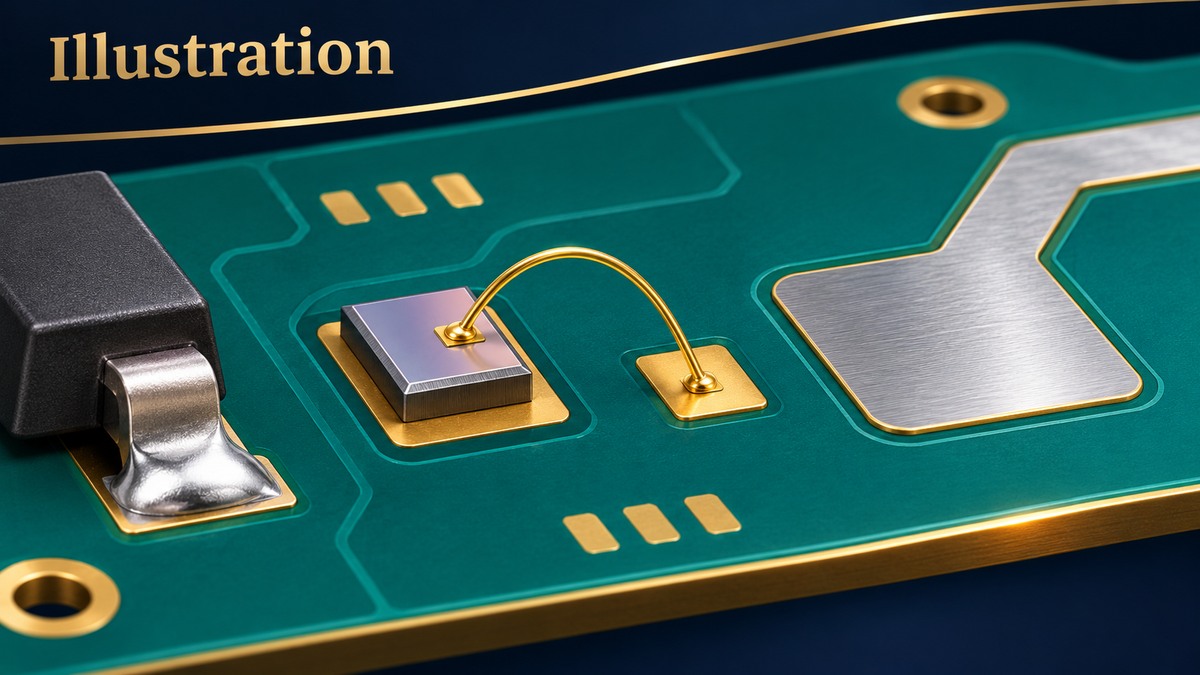
Table of Conent
Table of Conent
Choose ENIG, ENEPIG or immersion silver from the function of each exposed surface, then qualify the finish with the actual assembly process. Soldering, wire bonding, radio-frequency (RF) transmission and repeated contact mating require different evidence. A finish that solders well does not automatically provide the required bond strength, RF loss or contact life. Specify the complete deposit system, the relevant processing history and the acceptance method before releasing fabrication.
For a soldered assembly, compare the available qualified processes and handling requirements. Where wire bonding is present, identify the wire material and bonding method. Where RF performance matters, evaluate the actual plated geometry. Repeated-mating contacts need a separate wear specification and test plan.
Start with the function of each exposed pad
A pad-function map is more useful than a board-wide “premium finish” label. Mark solder lands, bond pads, RF conductors, test points and mating contacts. Some boards can use one qualified finish throughout; others need selective treatment or a revised interface. That decision should come from competing requirements, not the apparent color of the surface.
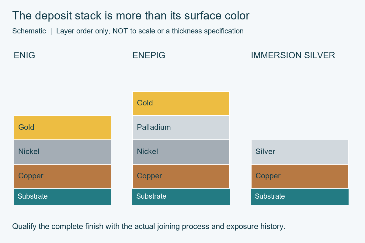
ENIG means electroless nickel with immersion gold. ENEPIG adds electroless palladium between the nickel and gold. Immersion silver deposits silver over exposed copper without the electroless nickel layer used in those two stacks. MacDermid Alpha’s immersion-silver description identifies that architecture and describes soldering, high-frequency and aluminum-wire-bonding applications for its processes. The last point matters: a generic comparison table saying that all immersion silver is unbondable is too broad.
| Interface | Question that controls selection | Evidence to obtain |
|---|---|---|
| Soldered component land | Will the finish support the specified alloy and complete thermal history? | Solderability and assembly results after representative storage and processing |
| Wire-bond pad | Which wire material, bond mode and prior process exposures apply? | Bond qualification with the actual deposit process and acceptance criteria |
| Exposed RF conductor | How does the finished geometry affect the allocated loss? | Comparable simulation or measurement of the relevant path |
| Repeated-mating contact | What wear, contact-resistance and environmental duty must be met? | A separately specified contact system and representative endurance evidence |
Record conflicting functions early. For example, an exposed conductor may need low loss while nearby pads need a proven bonding process. Ask whether one qualified construction meets both requirements before accepting the complexity of selective finishing. Include boundaries, registration and inspection access if different finishes are proposed.
Qualify the actual wire-bond process
Wire-bond suitability belongs to a material-and-process combination. State the wire material, diameter, bond method, substrate, pad geometry and acceptable failure modes. Include storage, cleaning and thermal exposures before bonding. A result on freshly plated pads may not represent pads that have passed through the full assembly route.
MacDermid Alpha’s Affinity ENEPIG information describes a specific nickel-palladium-gold process intended for soldering and wire bonding. That supports evaluating ENEPIG when both joining methods are required. It does not establish that every fabricator’s ENEPIG deposit will meet an arbitrary bond program. Ask which process, substrate and exposure history the supplier’s qualification actually covers.
Fraunhofer ISIT’s wafer-metallization discussion explains that an intermediate palladium layer can widen the process window for wire bonding in its application. Its wafer process is not a transferable PCB thickness specification. Use the underlying distinction to ask better questions about the actual bond interface rather than copying a deposition range into a board drawing.
ENIG should likewise be evaluated against the required bonding method rather than marked universally acceptable or unacceptable. Gold-wire and aluminum-wire processes are different questions. A supplier’s successful result for one should not silently authorize the other. Require the responsible bonding engineer to approve the process and define acceptance, including what happens when results fail or remain inconclusive.
Once the joining functions and process sequence are defined, share the pad-function map and assembly sequence with the board files, material constraints and required bond or soldering evidence. The review can align finish availability, assembly operations and sourcing assumptions before suppliers price different interpretations of the same drawing.
Evaluate RF loss on the finished construction
RF finish selection needs a path budget and a representative construction. Identify the plated conductors, transmission-line geometry, frequency range, finish extent, copper properties and measurement reference planes. A finish change may matter differently on different structures, so a universal frequency cutoff or loss penalty is an unreliable procurement rule.
The original ENIG modeling and measurement study by Rautio and Coonrod examines several PCB topologies and includes conductor side-wall plating. It reports frequency-dependent insertion-loss effects for its tested structures. The useful engineering lesson is to preserve the geometry and finish model when comparing alternatives; its experimental values should not become an allowance for an unrelated board.
Immersion silver is worth evaluating where a nickel-free exposed conductor helps the actual RF requirement. ENEPIG retains a nickel layer beneath its palladium and gold, so adding palladium should not be assumed to remove the RF consequences of the entire stack. Conversely, a measured ENIG path that meets its approved budget need not be changed solely because a generic chart ranks another finish higher.
Use the RF construction and measurement boundary to distinguish a uniform coupon from connector launches and populated circuitry. Compare alternatives using the same included path, setup and conditions. If the finish is selectively applied, verify that the test vehicle represents its location and coverage rather than only the underlying dielectric stackup.
Separate the finish effect from other changed variables. A comparison using different laminate thicknesses, trace widths or copper foils cannot isolate a finish contribution without further analysis. Retain the approved baseline and identify each change in the comparison record. The decision should show whether the complete path meets its requirement, not merely which sample has the lowest measured number.
Record whether the RF result applies to a bare finished board or to the final populated assembly. Soldering changes the local interface at component lands, and the finished signal path may include exposed and assembled regions. A bare-board comparison therefore supports only its stated boundary. Identify which result closes the final product requirement and which result is a diagnostic or process-development comparison.
Separate contact duty from solderability and storage
Repeated-mating contacts require their own functional definition. Specify the mating system, mechanical duty, environment, contact-resistance criterion and inspection or endurance method. Neither gold appearance nor a solderable finish name establishes a cycle rating. If a dedicated contact finish is needed, release that requirement separately from the solder lands and review any selective-process boundary.
Storage and handling also belong in the comparison. Obtain the exact finish supplier’s packaging, permitted exposure, storage and assembly instructions. Record manufacture and opening dates where required, resealing rules and the disposition for suspect or overexposed stock. Avoid adopting a generic shelf-life number as evidence that a particular lot remains assembly-ready.
Do not prescribe a universal bake or cleaning treatment for all three finishes. A recovery operation must be compatible with the finish, board materials, components already present and subsequent joining steps. Have engineering approve the route and define the evidence needed afterward. A visually bright surface is not, by itself, proof of solderability or bondability.
The official OrinewPCB overview below compares ENIG, HASL and OSP as general surface-finish choices. YouTube identifies it as AI-generated educational content. It provides selection context, rather than test evidence for ENEPIG, immersion silver or a specific production lot.
Release one finish specification and its evidence
A release-ready finish specification identifies the deposit system, applicable controlled requirements, approved process or substitution route, covered surfaces and acceptance responsibilities. Define layer-thickness requirements and measurement methods through the agreed specification. Keep qualification of the finish process separate from acceptance of the assembled product.
Uyemura’s ENEPIG process discussion is another example of a supplier addressing combined soldering and bonding applications. Such process information can support a shortlist. Purchase acceptance still needs the actual supplier’s controlled process evidence and the product’s requirements.
| Decision | Record to define | Boundary |
|---|---|---|
| Deposit conforms | Specified composition, layer measurements, sampling and lot traceability | Does not independently establish bond strength or RF performance |
| Joining process works | Representative solder or bond qualification and contracted production checks | Applies to the recorded materials and exposure history |
| Electrical or contact duty is met | RF path or contact evaluation under approved conditions | Does not authorize an unreviewed finish substitution |
Compare total process scope as well as finish price. Separate selective masking, handling, qualification samples, assembly sequencing and required supplier records. A lower unit finish charge may omit work that another quotation includes; reconcile those assumptions before making a purchasing decision.
Connect each decision to a requirement-to-test acceptance record. Within a full-turnkey PCB assembly scope, fabrication, sourcing, assembly and specified tests should use the same released finish and revision. Evaluate a finish, supplier or process change before relying on previous qualification.
The selection is complete when pad function, process history and acceptance evidence agree. For a project at that point, provide the controlled board and assembly files with the finish map, bill of materials, placement data, quantities, joining sequence and required tests. These inputs let the quotation review identify fabrication, sourcing, assembly and verification work against one consistent scope.
Latest Blog



Contact Info
Phone: +86-755-82882936
Email: [email protected]
WhatsApp: +86-13570802455
Wechat: +86-13570802455
Address: 2nd floor,D Bldg.,Electric Link Technology Bldg.,Gongming,Guangming New Dist.,518106 Shenzhen, China
