
PCB Copper Pours: Net Connectivity, Thermal Reliefs, and Release Checks
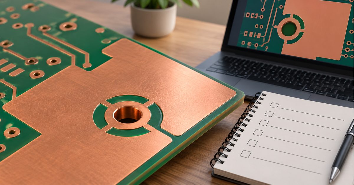
Table of Conent
Table of Conent
A PCB copper pour creates a copper region around the layout’s other features. It can support a defined electrical connection, but filling empty space with copper does not automatically produce a useful ground or power network. The assigned net, actual connected geometry, clearances, and pad connection style determine what the region does.
Review the final filled copper rather than only the polygon boundary. A pour can be divided by routing, reduced to narrow connections, or leave isolated areas that do not serve the intended net. This guide explains how to evaluate those conditions, choose connection styles deliberately, and release fabrication data that matches the reviewed layout.
Define the purpose and net before drawing the boundary
Start with the function of the region. Is it intended to connect a particular supply, provide a ground connection, or support another documented purpose? Specify the net in the design and confirm that the relevant pads and vias belong to it.
Altium’s polygon-pour introduction describes assigning a net and repouring the region to create the actual connected copper. The boundary is an instruction to the CAD tool; the resulting copper must still be inspected.
Do not assume a large colored area means a continuous electrical path. A same-net label is useful design information, but it does not prove that every separated piece has a physical connection. Trace the intended path through the filled geometry and use the applicable connectivity checks.
Keep special purposes explicit. A deliberate unconnected copper feature should not accidentally become the assumed return path for a signal or supply. Document why it exists and how it is treated in the design review.
Distinguish a solid connection from thermal relief
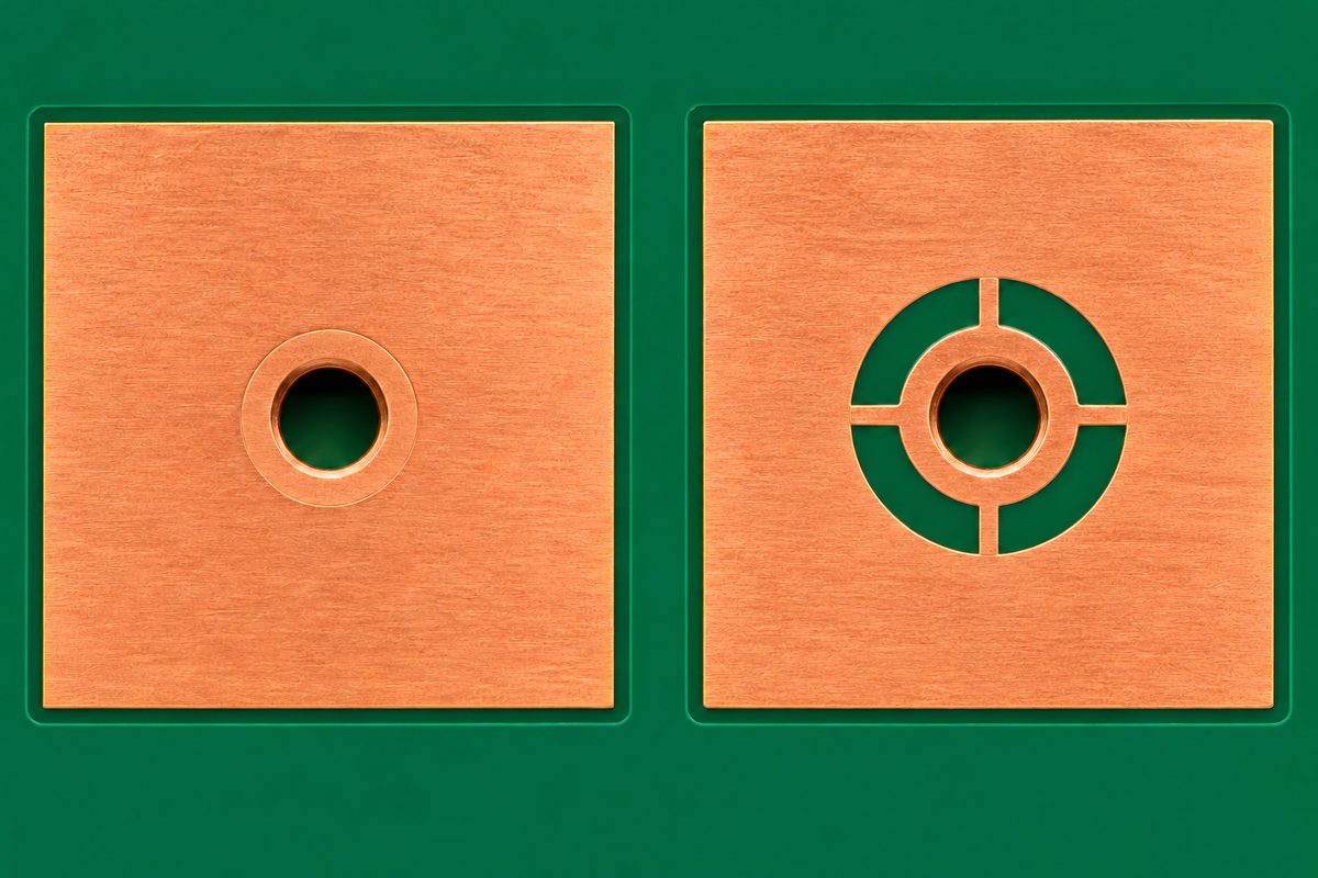
A solid connection joins the pad to the surrounding copper without the relief gap-and-spoke pattern. A thermal relief leaves a gap around much of the pad while connecting it through narrower copper spokes. The narrowed geometry changes heat transfer as well as the electrical connection.
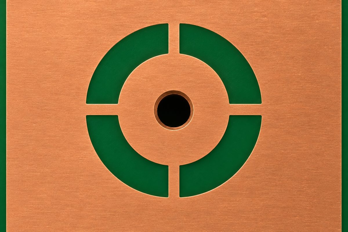
A relief can reduce the heat drawn away from a soldered pad into a large copper area. However, the selected connection must also meet the electrical and manufacturing requirements. It is not enough to choose thermal relief everywhere because it may make one soldering task easier.
Conversely, a solid connection can increase the coupling to the surrounding copper and change the assembly heating demand. Review the actual component, copper construction, and assembly method before treating direct connection as universally better.
The reflow soldering process guide provides assembly context. Pad connection geometry is one input to process planning, not a replacement for a suitable profile and the component’s requirements.
Evaluate spokes as real copper paths
The relief gap, spoke width, number, and placement determine the connection geometry. A drawing with four intended spokes is not enough if obstacles prevent some from reaching the surrounding region after fill.
KiCad’s PCB Editor documentation distinguishes the thermal gap from spoke width and includes checks for incomplete relief connections. Inspect the resolved copper, especially around nearby pads, traces, and zone boundaries.
In a hypothetical design example, a connector pad may have four requested spokes but only two that can connect because adjacent clearance areas block the others. The required response is to review the actual connection and applicable rules, not simply to count the spokes visible in the pad’s settings dialog.
For a current-carrying connection, consider the remaining paths, copper thickness, geometry, operating conditions, and allowable temperature rise. Do not assign a universal current rating from spoke width alone. A narrow connection can dominate the path even when the surrounding pour is large.
When assembly heating and current requirements compete, send the relevant layout, copper construction, component requirements, and assembly method for an engineering and quotation review. Identify the affected pads so the discussion can address a specific connection rather than changing every pad globally.
Check rule scopes and local overrides
Connection settings may be inherited from board rules, zone properties, footprints, or individual pad configuration. A global setting does not necessarily control a pad that has an intentional or forgotten override.
Altium’s custom pad-stack documentation explains that pad-level thermal relief settings can override the applicable polygon connection rule. It also describes repouring when changed settings are not applied automatically. Review both the source settings and the resulting geometry.
For unusual pads, check the intended connection points instead of assuming a standard circular pattern. An elongated or custom-shaped land may require a different review from an ordinary through-hole pad. Preserve the component’s relevant footprint and manufacturing requirements.
After editing a library or moving between software versions, refill and rerun checks before export. Do not assume that the old on-screen fill remains a valid representation of the new rules. Record any exceptional pad settings in the review notes so another engineer can understand why they differ.
Inspect islands, necks, and interruptions
Routing and clearance boundaries can split a region into separate pieces. Inspect whether each piece has the required connection and whether that path remains suitable after later layout changes.
KiCad documents controls for removing isolated copper areas, with behavior depending on the zone’s configuration. Use the feature deliberately, then inspect the result. A removal setting is not a substitute for checking that the remaining copper supports the intended connection.
Also inspect narrow necks between larger copper areas. A region may be connected geometrically while carrying the intended current through an unexpectedly small path. Review the complete route from source to load rather than only the area adjacent to a pad.
If a copper region is meant to support a signal reference, examine the actual return-path context. Avoid blanket claims that additional copper automatically improves noise or electromagnetic performance. Interruptions, net relationships, and routing geometry require a design-specific assessment.
Choose solid or hatched fill for a reason
A hatched fill leaves a pattern of copper segments instead of a continuous solid area. It changes the copper geometry and available connection paths. Select it because the construction and function call for it, not because its preview looks cleaner.
Do not transfer settings between rigid and flexible constructions without review. Likewise, do not assume equal outer dimensions make a hatched region equivalent to a solid one for current, shielding, or heat spreading. The relevant engineering assessment should use the actual geometry.
Confirm that the hatch segments, gaps, and local connections can be fabricated for the selected copper construction. Inspect the exported artwork, because the manufacturing recipient sees the generated copper pattern, not the CAD boundary and its styling controls.
Use the PCB manufacturing capabilities page as a starting point, then confirm the copper geometry and construction required by the actual order. A generic capability listing does not approve every relief or hatch configuration.
Refill, check, and export in that order
Perform a controlled refill after the layout and rules are ready. Review changed regions, run the relevant clearance and connectivity checks, and resolve exceptions before generating fabrication files.
The CAD manufacturing-file checklist explains why the exported package needs its own review. Compare the copper images with the geometry approved in the design, including a representative solid connection, thermal relief, and dense routing area.
Use the same release revision for copper, drill data, outline, stackup, and drawing requirements. If a last-minute change modifies a polygon or pad, regenerate the affected package rather than mixing new copper with older companion files.
For an unresolved copper connection, submit the exported copper layers, drill data, stackup, and marked pad locations for a fabrication review. State the intended connection and any acceptance requirement so the review can distinguish an export problem from a design choice.
Investigate soldering findings with evidence
If an assembly pad does not wet or heat as expected, do not immediately conclude that its relief is the cause. Collect the board revision, component identification, observed condition, process information, and the actual copper geometry.
Compare affected and unaffected locations while considering differences in construction and assembly conditions. A layout change that adds or removes spokes should address an identified issue and still preserve the electrical function. Do not increase heating or alter copper simply to mask an unexplained defect.
For a revised build, define how the change will be reviewed and what evidence will confirm the intended result. A successful solder joint at one location is useful evidence for that location, not automatic validation of every changed connection on the board.
Release checklist
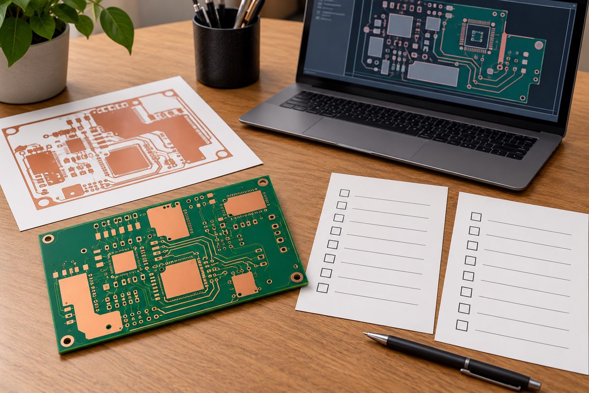
- Assign and verify the intended net and region function.
- Choose connection styles for the actual electrical and assembly needs.
- Inspect resolved spokes, narrow necks, and separated copper areas.
- Review scoped rules and pad or footprint overrides.
- Confirm fabrication suitability of the actual copper geometry.
- Refill, run checks, and compare exported copper with the approved layout.
- Keep the release files and exception notes at one revision.
Preparing production? send the final fabrication package, BOM, quantities, assembly method, and critical connection requirements for review and quotation. A useful copper pour is one whose actual paths, rules, and released images support the documented purpose—not simply one that covers the most board area.
Latest Blog

Contact Info
Phone: +86-755-82882936
Email: [email protected]
WhatsApp: +86-13570802455
Wechat: +86-13570802455
Address: 2nd floor,D Bldg.,Electric Link Technology Bldg.,Gongming,Guangming New Dist.,518106 Shenzhen, China