
PCB Gold-Finger Beveling: Geometry, Fit, and Drawing Checks
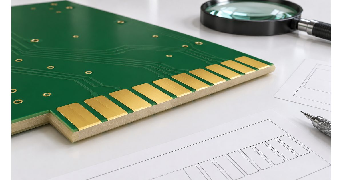
Table of Conent
Table of Conent
PCB gold-finger beveling shapes the leading edge of a card so it can enter its mating connector with the intended mechanical interface. The gold contacts, board thickness, bevel, and connector geometry must work together. Specifying only a bevel angle leaves important questions unanswered, including the remaining tip thickness, the length of the machined region, and its relationship to usable contact area.
Start with the selected connector’s current drawing and application requirements, then translate those requirements into a controlled PCB drawing. This guide focuses on that translation and the manufacturing checks that support it. It does not prescribe one universal angle, copper setback, plating thickness, or insertion-force limit.
Use the connector interface as the starting point
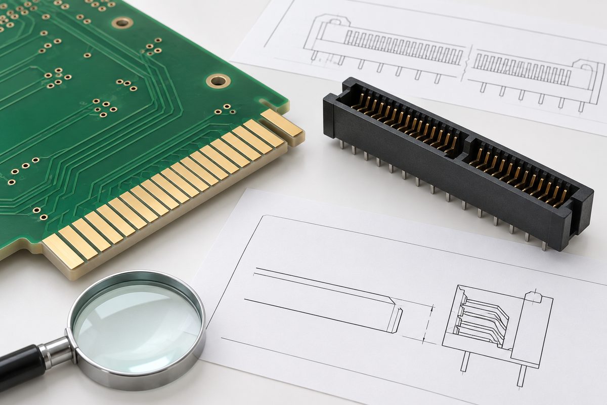
Identify the exact mating connector and the documentation revision used for design. Check the permitted card thickness, edge profile, insertion depth, contact pattern, keying features, and relevant tolerances. A generic edge-card outline is not enough to approve a particular connector combination.
As one example of the documentation hierarchy, TE Connectivity’s card-edge connector product page directs designers to the product drawing for design activity and provides separate application and product documents. That is an example of where requirements are found, not a recommendation to select that connector or transfer its dimensions to another family.
Review fit with the complete mechanical assembly. The card may be constrained by guides, a bracket, a housing, or adjacent boards before it reaches the socket. A correct bevel cannot compensate for a misplaced board stop or a connector whose alignment differs from the intended insertion path.
Dimension a cross section, not an isolated angle
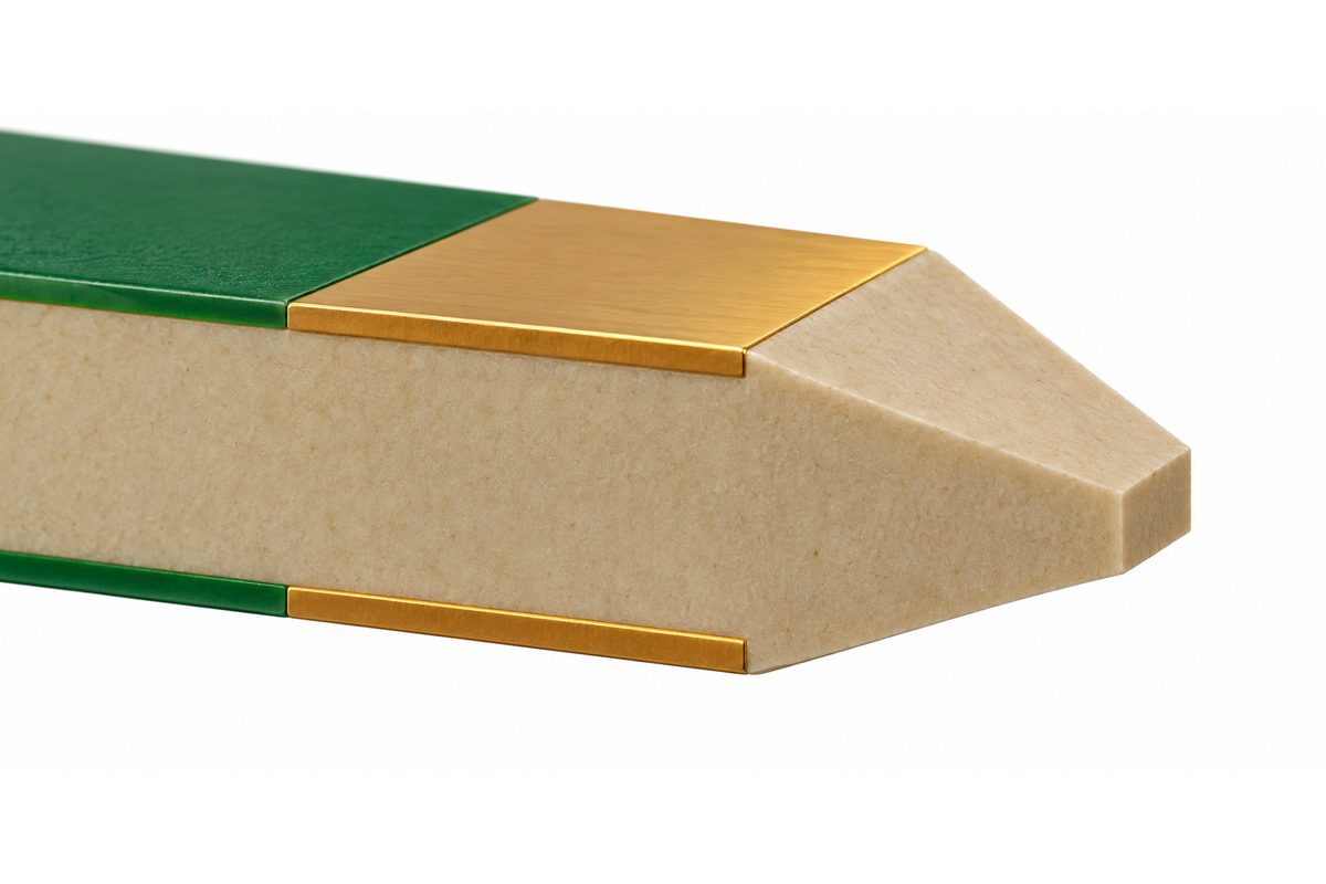
A bevel describes an angled removal of material, but the angle needs an explicit reference. Show the finished board faces and leading edge in a sectional detail. State whether both sides are machined and whether the profile is symmetric. Avoid relying on a note that can be interpreted as an included angle or an angle measured from a different face.
Define enough geometry to establish the intended profile without creating conflicting dimensions. Relevant attributes include finished card thickness, the remaining leading-edge thickness, bevel extent, and the angle convention. Where dimensions are dependent, distinguish controlling dimensions from reference information and provide a coherent tolerance scheme.
For a symmetric idealized profile, changing the remaining tip thickness at a fixed board thickness changes how much material is removed from each face. Changing the angle changes the distance over which that removal occurs. This geometric relationship is why two drawings with the same angle can produce different entry profiles.
Coordinate the card-thickness requirement with the PCB thickness and connector-fit guide. Determine what the applicable thickness dimension includes and where it is to be assessed. A stackup nominal is useful for planning but is not a substitute for the finished-interface requirement.
Protect the usable contact region
Locate the gold-finger pattern relative to the controlled board profile and connector interface. Confirm the required contact width, pitch, usable length, and position from the applicable drawing. Review how the bevel boundary relates to the contact area rather than assuming every visible gold surface is available for mating.
A chamfer can remove material near the leading edge. Do not extend it arbitrarily farther into the contact region to make insertion feel easier. The finished profile must still support the intended engagement, wipe, and seating arrangement. Ask the connector and PCB engineering teams to resolve any conflict between the mating requirement and a proposed manufacturing change.
If the design includes shorter contacts for a defined mating sequence, preserve that geometry and its electrical intent. Do not normalize finger lengths during artwork cleanup. Document such features clearly enough that the fabricator can distinguish them from an accidental pad-length difference.
Have an unresolved fit or contact-area question? send the connector drawing, card profile, stackup, contact artwork, and marked bevel requirements for engineering review. Identify the required interface so the geometry can be assessed before quotation.
Keep internal copper out of the machined envelope
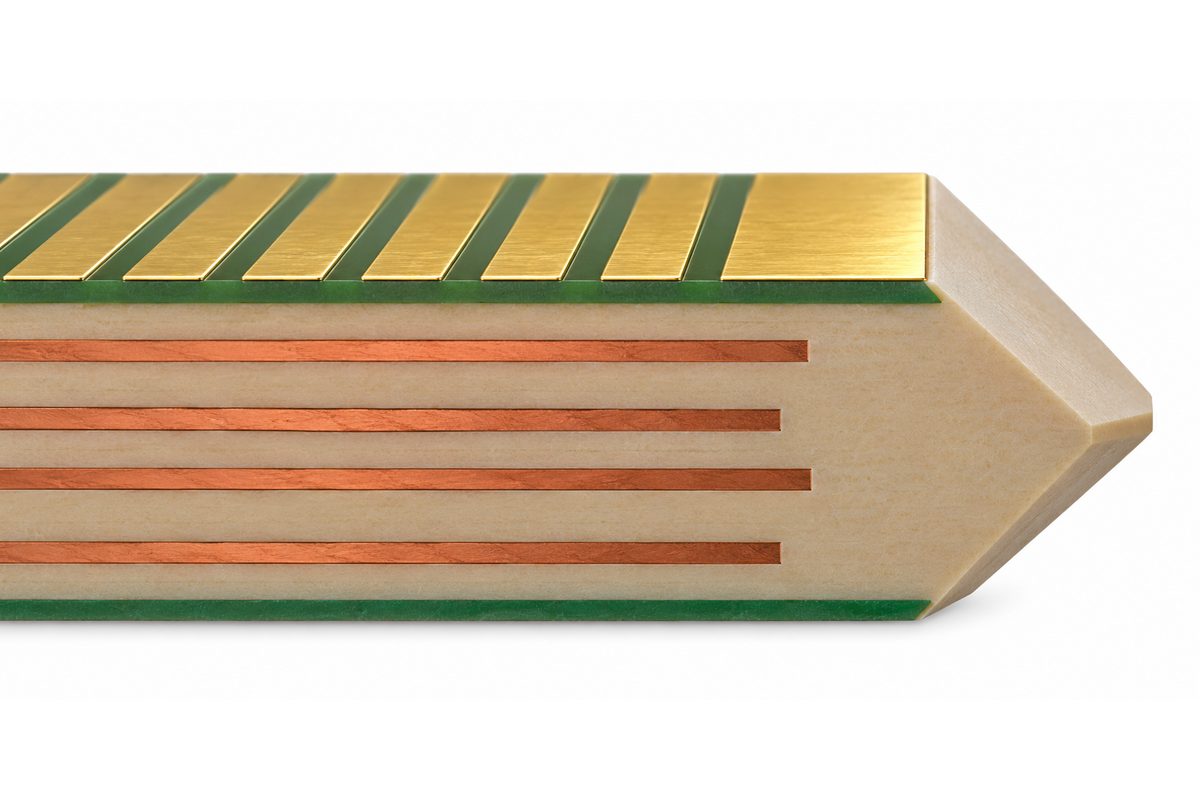
Beveling cuts into the laminate near the board edge. Internal copper that reaches the cut region can become exposed. Review all affected layers, including plane fills and features that are not obvious in a top-side screenshot.
Eurocircuits’ edge-connector design guidelines relate bevel geometry to inner-layer copper clearance and describe different machining arrangements. Its clearance values and equipment constraints are supplier-specific. Use the principle to request a review of your actual cross section, rather than treating its table as an assypcb.com capability specification.
Establish the copper-free region using the finished profile, intended material removal, and agreed manufacturing tolerances. Include uncertainty in profile position and machining, not only the nominal chamfer line. A two-dimensional clearance from an unmachined edge may not describe the complete three-dimensional risk.
Keep electrical requirements in view. Moving a reference plane or nearby conductor can affect the design, so do not accept an expanded copper setback without engineering review. Reconcile the machining envelope with the electrical layout before freezing production files.
Separate beveling from the contact finish
The bevel is a mechanical feature; the contact finish is a separate surface requirement. A gold-colored rendering does not define plating composition, thickness, underplate, wear performance, or inspection acceptance. State the required finish independently and verify its suitability for the mating application.
Eurocircuits’ edge-contact gold-plating overview distinguishes hard plated gold for repeatedly mated contacts from an immersion-gold board finish. It also explains why plating connections and panel access affect the production route. Its materials, thicknesses, and processing sequence should not be generalized to another manufacturer.
Specify the contact region and the finish for the rest of the board without ambiguity. Ask how temporary plating connections will be handled and whether the final profile removes them as intended. Do not assume a bevel instruction automatically selects a contact finish or includes all finishing operations.
Review machining access and panel delivery
A bevel on a simple accessible outer edge may need a different route from one beside an internal notch or on boards delivered in a panel. Confirm which edges are to be beveled, their start and stop locations, and the condition in which the supplier will perform the operation.
Keep break tabs, rails, and nearby features out of the way of the required machining access. If panel delivery is necessary for assembly, ask the fabricator and assembler to coordinate the bevel and separation sequence. A drawing that is feasible for an individual board may not describe a feasible delivered panel.
The PCB slots and routed-feature guide provides context for notches, keying features, and controlled contours. Bevel information should supplement that geometry, not create a second conflicting board outline on another layer.
Review the proposed construction against the PCB manufacturing capabilities, then request project-specific confirmation. A general capability page does not approve every edge location, bevel profile, contact finish, or customer-panel arrangement.
Comparing manufacturing options? submit the individual-board and panel drawings, bevel locations, contact-finish requirements, and quantities for manufacturing review and quotation. Ask that the quote identify its machining and delivery assumptions.
Make the drawing and production data agree
Use one controlled revision for the board profile, copper artwork, stackup, mechanical detail, and connector reference. Identify the relevant drawing section and the edges it applies to. Include a clear datum scheme so contact position, keying, and machined geometry share a consistent reference.
As a hypothetical example, “bevel gold fingers” on an order form leaves the supplier to infer the profile and scope. A better package identifies the mating connector, affected edge, sectional geometry, controlling tolerances, copper-free region, finish, and required approval of deviations. This is a documentation framework, not a complete fabrication note.
Agree on who may change the profile or clearance and which changes require approval. Preserve the accepted drawing and any supplier clarification with the order. Reusing an older quotation without its geometry assumptions can recreate an ambiguity on a repeat build.
Verify geometry and mating as different checks
Agree on dimensional and visual inspection requirements before manufacture. Relevant evidence may include the finished card thickness, sectional profile, affected edge location, copper exposure, and contact condition. Choose methods that can assess the specified attributes, rather than relying only on a photograph.
A mating trial with the intended connector provides useful assembly evidence but does not replace dimensional acceptance or finish verification. Likewise, a dimensional pass does not prove the complete product’s insertion, retention, or repeated-mating performance. Validate each requirement with the appropriate evidence and conditions.
If a problem appears, record the board and connector revisions, lot information, observed location, and test setup. Compare the actual profile with the accepted drawing before changing an angle or contact length. Avoid fixing one symptom by introducing an unreviewed change elsewhere in the interface.
Pre-release checklist
- Confirm the mating connector and current application documents.
- Define card thickness, bevel reference, remaining tip, scope, and tolerances coherently.
- Protect the usable contact region and any intentionally shorter fingers.
- Check internal copper against the full machining envelope.
- Specify contact finish separately and confirm panel and machining access.
- Freeze matching production data and agree on inspection and mating evidence.
PCB gold-finger beveling is an interface-control task, not just an angle selection. A clear section, consistent contact geometry, protected internal copper, and agreed manufacturing route give the supplier a workable definition of the finished edge.
Ready for fabrication? submit the final artwork, stackup, sectional bevel drawing, connector documentation, quantities, and inspection requirements for engineering review and quotation. Resolve deviations before releasing the manufacturing package.
Latest Blog

Contact Info
Phone: +86-755-82882936
Email: [email protected]
WhatsApp: +86-13570802455
Wechat: +86-13570802455
Address: 2nd floor,D Bldg.,Electric Link Technology Bldg.,Gongming,Guangming New Dist.,518106 Shenzhen, China