
PCB Teardrops: Pad Transitions, Clearance, and Release Checks

Table of Conent
Table of Conent
PCB teardrops add copper at the junction where a narrow trace meets a pad, via, or another copper feature. The transition widens gradually instead of leaving the entire connection concentrated at a narrow entry point. The added geometry can provide useful local margin, but it does not replace adequate pad dimensions, fabrication clearances, or a reviewed electrical design.
Use teardrops to address a defined connection concern rather than enabling them globally without inspection. The practical review includes where they are added, how much copper they introduce, which neighboring features constrain them, and whether the final fabrication files preserve the intended result.
Identify the connection being reinforced
Do not confuse a teardrop with a thermal-relief connection. A teardrop widens a local junction; a thermal relief separates a pad from surrounding copper except for selected spokes. They answer different design questions. Review each actual copper path independently, especially when a trace entry and a polygon connection share the same pad. Adding a taper must not silently bridge an intended relief gap or create an unintended connection.
A teardrop is copper geometry, not a solder mask shape or a change to the drilled opening. At a round pad, it commonly broadens the trace as it approaches the land. Other transitions can involve surface-mount pads or a change between trace widths.
Autodesk’s teardrop overview describes these connection types and configurable width and length. The feature should be assessed in relation to the actual junction, not merely the familiar tapered shape.
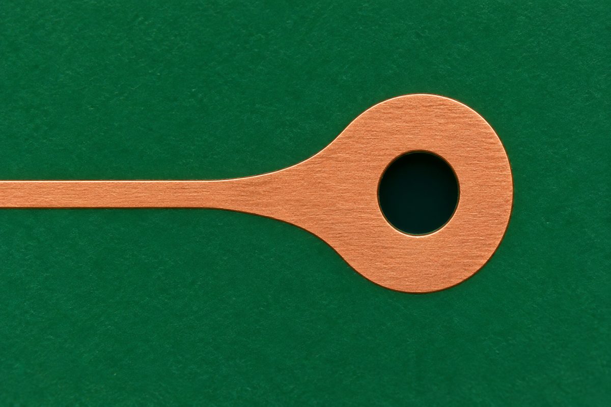
For a drilled pad or via, consider the trace entry direction and the applicable drill-to-copper relationship. A widened entry can leave more copper near that junction, but the hole and land still need to meet their requirements on the relevant layers.
Our PCB annular-ring design guide explains the distinction between nominal geometry and minimum remaining copper. A teardrop on one side of a pad does not establish the required ring around the entire opening.
Understand the benefit without overstating it
Altium’s teardrop documentation explains why drill misalignment can remove copper near a narrow track-to-pad connection. Adding a transition can strengthen that local geometry, especially where design objects are small.
That does not mean a teardrop prevents every breakout or makes an otherwise unacceptable feature compliant. The actual opening, land size, registration, and governing requirements remain relevant. Do not use a visual reinforcement to waive an unresolved fabrication rule.
Similarly, avoid promising a fixed improvement in yield or reliability without evidence from the particular construction and process. A geometric change is a design input. Its benefit depends on the condition being addressed and the board’s requirements.
For a design with a known vulnerable connection, document the concern and the intended change. A targeted review is more useful than the statement that teardrops are always required or always unnecessary.
Choose scope before choosing size
Group candidate sites by function and geometry. Narrow traces entering drilled pads may require a different assessment from surface-mount pad entries or trace-width transitions. Start with locations that have an identified concern rather than assuming all connections should receive the same shape.
In a hypothetical example, a fine trace entering a round via in open space might allow a useful taper. A nearby pad in a dense connector row could prevent the same taper from meeting clearance requirements. Applying identical settings to both locations would ignore their different constraints.

Keep exceptions visible in the review. If a connection is intentionally excluded, identify whether the reason is clearance, electrical behavior, a component requirement, or another documented constraint. Do not treat the absence of a generated feature as proof that the software approved the original junction.
If the appropriate scope is unclear, send the copper layers, drill data, stackup, and marked connection locations for a fabrication review. Describe the issue that the proposed reinforcement is intended to address.
Review the surrounding clearance after addition
Added copper occupies space. Check its relationship to neighboring pads, traces, vias, and board features after generation. A transition that merges neatly into its own net can still approach copper on another net too closely.
Do not force a feature through a clearance violation simply to make the connection look stronger. Altium documents options that can force teardrops or adjust their size to fit rules. The release decision should be based on the resulting geometry and applicable constraints, not the convenience of a generation option.
If a taper is reduced substantially to avoid an obstacle, inspect what remains. Confirm that it still addresses the intended concern, and assess whether moving the entry or changing the local routing is the more suitable response.
Also inspect solder mask and assembly-facing requirements when copper changes affect a surface pad. A copper transition is not permission to enlarge the mask opening or alter the component’s recommended land pattern without review.
Keep electrical requirements in the assessment
The added region changes local conductor geometry. For a controlled-impedance or otherwise sensitive path, review the transition in the context of the applicable electrical requirements. Do not assume that a visually smoother taper automatically improves signal performance.
For a current-carrying connection, a larger junction does not remove every narrow section elsewhere in the route. Review the complete path and copper construction. Do not assign a current rating from the teardrop’s appearance or maximum width alone.
Flex and other mechanically demanding designs require construction-specific review. Local reinforcement may be relevant, but bending location, materials, and the complete interconnect geometry still matter. Avoid copying a rigid-board setting into a flex design as if it were a qualification rule.
Use the PCB manufacturing capabilities page as a starting point, then confirm the actual construction and geometry being ordered. A generic capability table does not approve a particular taper or waive an electrical requirement.
Assign responsibility between CAD and CAM
Decide whether the released design already includes teardrops and whether any supplier-side modification is permitted. Do not leave both teams independently adding geometry to the same connections without agreement.
Altium’s CAM additional-tools documentation cautions against adding teardrops in both the PCB editor and CAMtastic. This illustrates a broader release principle: one controlled source should define the approved result.
If the supplier proposes an addition in CAM, ask for a clear description or comparison of the affected locations. Review changes against clearance and design intent before approval. Preserve the original package and identify which modified data is authorized for manufacture.
For a supplier-proposed change, request a review with the original artwork, proposed connection changes, and critical electrical or clearance requirements. Tie the response to the board revision rather than accepting a general statement that reinforcement is routine.
Regenerate after routing edits and inspect the export
Teardrop behavior depends on the design tool and workflow. Moving a pad or changing a trace can affect generated geometry. Check the relevant software behavior and regenerate or update the transitions when required.
A preview before the final routing edit is not sufficient release evidence. Review the completed board, refill relevant copper, rerun checks, and inspect the actual exported layers. Do not assume a generation command succeeded at every intended site.
If a tool provides a generation report, compare it with the selected scope. Identify failed or omitted locations and resolve their cause. A count of visited objects is not necessarily a count of satisfactory transitions.
Our Gerber X2 release-check guide explains why the artwork and supporting information need their own inspection. Metadata cannot substitute for verifying that the copper transition appears correctly in the released image.
Evaluate a finding before changing the entire board
If a connection defect is observed, preserve the board revision, layer, feature location, and available dimensional or inspection evidence. Compare the finding with the released copper and hole data before selecting a corrective action.
Distinguish a design margin concern from a manufacturing variation, an export discrepancy, or damage introduced later. These can produce superficially similar observations but require different responses. Adding copper everywhere may obscure rather than resolve the original cause.
For a proposed revision, document which sites change and why. Recheck dependent requirements and agree on how the next build will be evaluated. Do not present a successful result at one modified feature as proof of every connection on the board.
Pre-release checklist
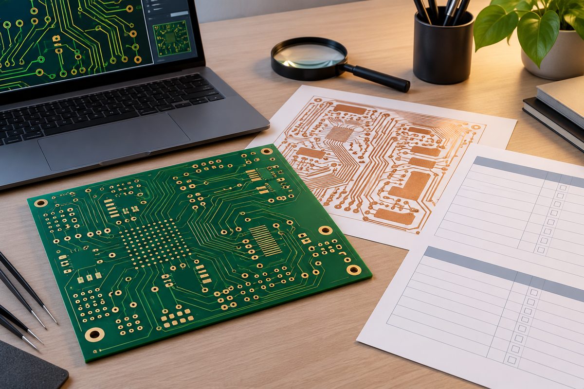
- Identify the connection concern and relevant feature types.
- Confirm pad, hole, and copper requirements independently.
- Review generated tapers against neighboring copper and other constraints.
- Check electrical and construction-specific effects where relevant.
- Define responsibility for CAD and supplier-side changes.
- Update features after routing edits and inspect generation exceptions.
- Compare final exported copper with the approved design.
- Keep revision and approval notes aligned with the fabrication package.
Preparing production? submit the final copper and drill files, stackup, quantities, and marked critical connections for review and quotation. A useful teardrop is a verified local transition that supports the documented requirements—not a blanket substitute for adequate pad geometry or process evidence.
Latest Blog


Contact Info
Phone: +86-755-82882936
Email: [email protected]
WhatsApp: +86-13570802455
Wechat: +86-13570802455
Address: 2nd floor,D Bldg.,Electric Link Technology Bldg.,Gongming,Guangming New Dist.,518106 Shenzhen, China