
PCB Via Tenting: Solder Mask Openings and Release Checks
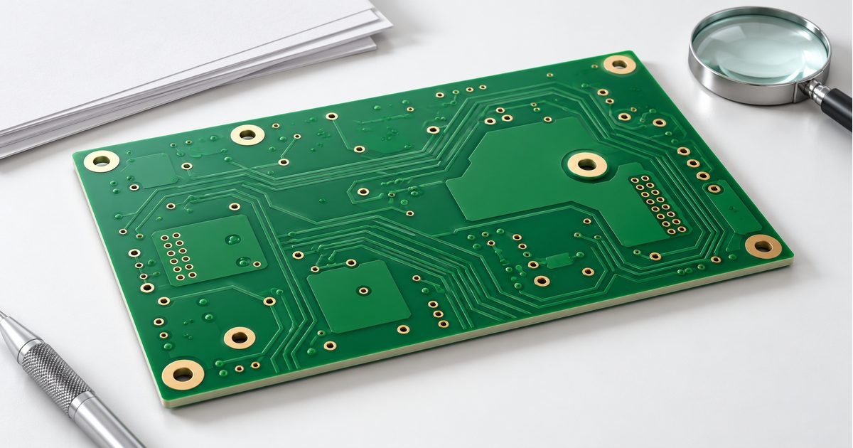
Table of Conent
Table of Conent
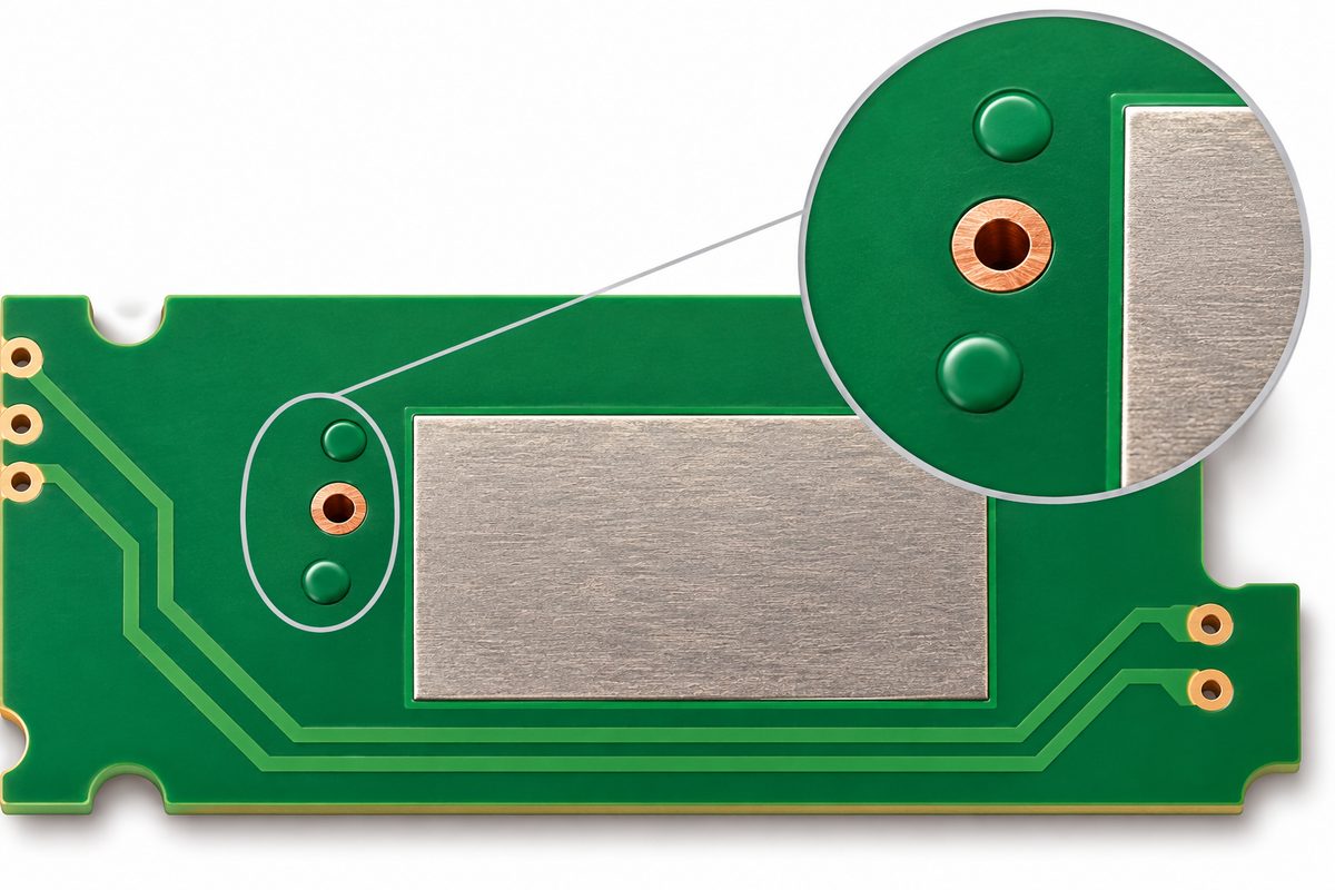
PCB via tenting uses solder mask to bridge a via opening instead of deliberately exposing it. For an ordinary routing via, that can help keep nearby soldering areas separate from an unwanted opening. However, a CAD setting that removes an opening from the solder-mask artwork does not establish that the manufactured hole will be reliably closed.
Start with the function you need: covering exposed copper, excluding solder, preserving a test contact, or producing a solderable land. Those are different requirements. This guide focuses on mask treatment of non-component vias and the release checks needed to communicate that treatment. It does not treat a tented hole as a substitute for a specified filled-and-capped via-in-pad structure.
Separate the artwork instruction from the finished structure
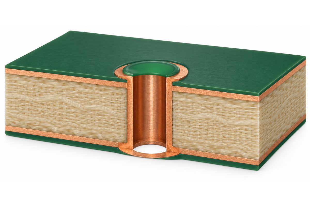
In layout data, a tenting option usually controls whether the solder-mask layer contains an opening at a selected via. In fabrication, the result depends on the mask material and application process. Keep these two meanings separate during engineering review: “no mask opening in the data” describes geometry, while “a closed tent after manufacture” describes a physical result.
Würth Elektronik’s via-protection design guide distinguishes a mask bridge over a hole from material that partly enters or fills the hole. Its supplier-specific offerings are not universal process capabilities. Use that distinction to ask the selected manufacturer what your artwork will actually produce.
Do not describe every green-covered via as filled. Nor should “covered” be taken to mean copper-capped. If the requirement is merely no intentional mask clearance around ordinary vias, state that clearly. If closure is functionally necessary, identify the affected holes and ask for a qualified construction and acceptance method.
Decide which vias should remain accessible
Before applying a board-wide rule, classify the exceptions. An assembly test contact, a programming connection, or a planned rework access point may need exposed metal. A routing via that happens to sit in a convenient location is not automatically an approved test point. Confirm its intended use with the team responsible for the fixture and service strategy.
Also distinguish vias from plated component holes. A connector lead needs an appropriate opening and soldering interface; it should not inherit a blanket rule intended for routing vias. Check footprint objects and imported layouts carefully, particularly when conversion between pad and via objects has occurred.
For exposed thermal pads and dense packages, consult the package land-pattern and assembly requirements. Mask coverage near a pad, mask over a hole, and a solderable surface over a filled hole answer different questions. The via-in-pad construction guide addresses the separate case where the via occupies the component land itself.
Review the top and bottom sides independently
A through-via can have different requirements on its two surfaces. The component side may be near an exposed solder land, while the opposite side may carry a test contact or another component. Record the intended top and bottom treatment rather than relying on a single unchecked “tent vias” instruction.
One-sided coverage is not automatically safer or more manufacturable than two-sided coverage. The actual processing sequence, surface finish, cleaning, and application method matter. Eurocircuits’ via-covering overview explains that different mask processes produce different results and that contaminants can become trapped in protected structures. Its process choice should not be generalized to all fabricators.
Ask the supplier to review the entire construction when a closed opening is required. Avoid selecting the number of covered sides solely from a layout preview. If contamination or sealing is an important concern, define the use condition and required evidence rather than assuming a mask tent provides a hermetic barrier.
Have a side-specific requirement that remains unresolved? Send the copper, drill and mask layers, marked via locations, and required side treatment for engineering review. Include the assembly purpose so the proposed approach can be evaluated before quotation.
Check mask openings, not just via properties
Altium’s pad and via documentation describes tenting through mask-expansion controls and object-level settings. The important release lesson is that a rule and an individual override can produce different outputs. Inspect the resulting artwork, not only the default value shown in the design rules.
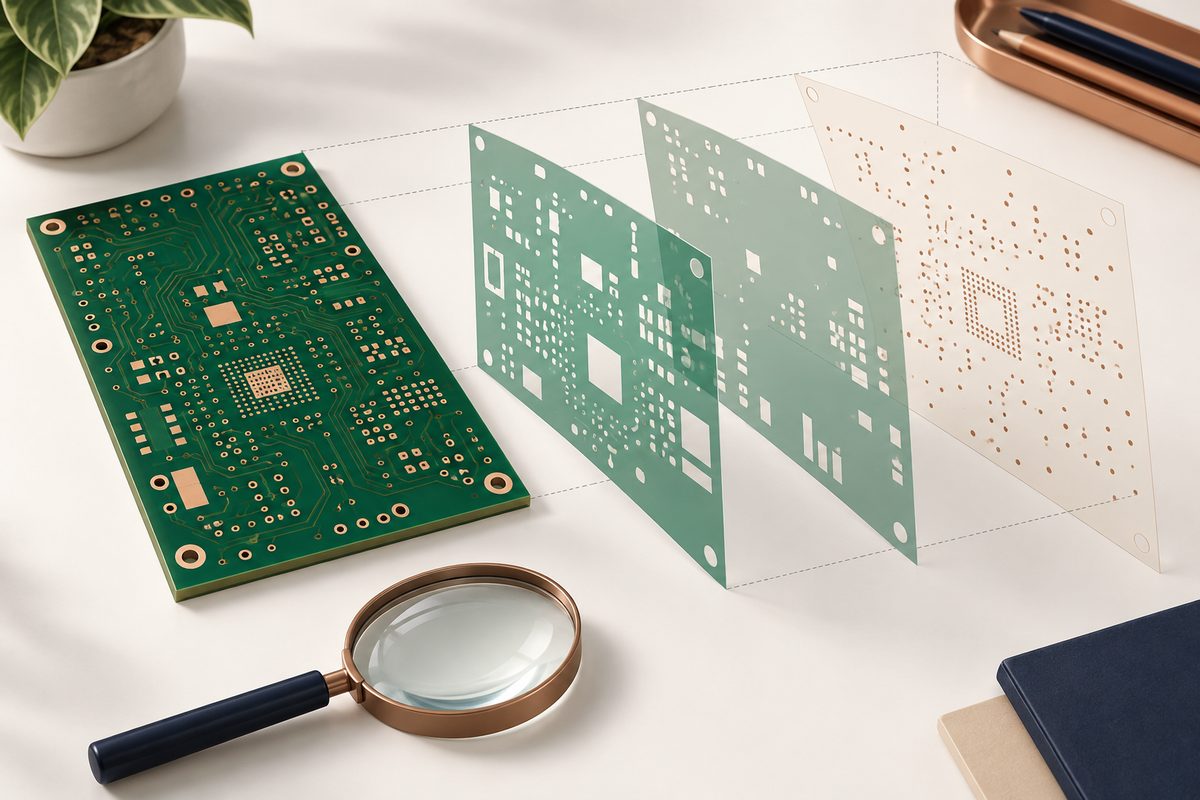
Use a fresh export after changes. Overlay each mask layer with its corresponding outer copper and drill information in an independent viewer. Identify whether the displayed shapes represent openings or coverage in that viewer. A reversed interpretation can make an apparently correct screenshot misleading.
Sample several via sizes, repeated regions, test exceptions, and imported footprints. A rule that works on one selected via may not cover another class or an overridden object. If the design has stitched or shielded via arrays, include them in the review rather than assuming generated objects inherited the intended settings.
The solder-mask openings and dams guide provides broader context for adjacent lands and mask webs. Here, concentrate on the particular boundary around each affected via and the neighboring solderable feature. Do not enlarge or merge openings simply to make the viewer display look cleaner.
Do not use a universal maximum tenting diameter
A published hole-size recommendation from one manufacturer reflects that manufacturer’s material, equipment, application method, and ordering conditions. It is not a transferable guarantee. Ask whether the quoted dimension describes the drill tool, finished hole, or another feature, and whether the recommendation applies to your board construction.
For a required closed tent, request the supplier’s relevant capability range and how closure will be inspected. If it cannot support the requirement, evaluate an agreed alternative or revise the design. Do not silently replace a critical closure requirement with “best effort” mask coverage because a prototype appeared acceptable.
Review the PCB manufacturing capabilities as a starting point, then flag the actual via geometry and mask requirement for project-specific confirmation. A general capability page does not approve every tenting, plugging, filling, or capping combination.
Specify the exceptions in the release package
Use a consistent selection method for vias with special requirements. Depending on the supplier’s approved data workflow, that might be a clearly identified drawing region, a selection layer, or explicit feature coordinates. Keep the selection synchronized with the final hole locations; an older marked screenshot can point to a different feature after routing changes.
A useful release package states the board revision, stackup, drill definitions, mask layers, surface finish, intended side treatment, and exceptions. Add the reason for any functional closure requirement and the agreed acceptance reference. Specify which changes require approval before the supplier modifies mask artwork or substitutes a process.
For example, an ordinary routing region might require no intentional top-side mask openings while dedicated test contacts remain exposed. That is an example of selection logic, not a complete fabrication note. A real order still needs the actual feature identification, opposite-side requirements, and supplier confirmation.
Comparing fabrication options? Submit the proposed via-treatment alternatives, released files, quantity, and inspection needs for a manufacturing and quotation review. Compare the same required result, not just two differently named order options.
Verify the result against the requirement
For first articles, distinguish data verification from physical inspection. Artwork review can establish that an intentional opening is absent. Surface inspection can document visible mask coverage. Neither alone proves internal fill, cap construction, cleanliness inside the barrel, or long-term behavior.
Agree on what evidence is appropriate before manufacture. If the requirement concerns only mask geometry, inspect that geometry. If it concerns closure or another functional property, define a suitable inspection or test with the supplier. A passing connectivity test does not prove a mask-related requirement has been met.
If a tent is damaged or an opening appears where none was expected, record the location, board revision, lot, side, and inspection conditions. Compare the observation with the released data and agreed acceptance requirement. Investigate before attributing it to a particular material or process step.
Pre-release checklist
On repeat orders, check that the accepted mask interpretation remains attached to the same revision and supplier route. Changing the mask color, finish, board supplier, or application process can justify another review even when the CAD geometry has not changed. Preserve the decision record with the released package.
- Confirm which features are routing vias, component holes, test contacts, or via-in-pad structures.
- State top and bottom treatment independently, including all exceptions.
- Separate no intentional mask opening from a required physical closure.
- Inspect fresh mask exports against copper and drill layers in a consistent viewer.
- Confirm supplier feasibility and agree on evidence for functional requirements.
- Freeze one revision for artwork, drawings, selection information, and quotation assumptions.
PCB via tenting works best as a deliberate mask and manufacturing decision, not a blanket preference. Preserve necessary access, verify the exported openings, and make any closure requirement explicit. That approach gives engineering, purchasing, and the fabricator a shared basis for deciding what the board must contain.
Ready to release the board? Submit the final fabrication files, marked exceptions, side-specific mask requirements, quantities, and acceptance needs for engineering review and quotation. Include unresolved questions before the manufacturing package is frozen.
Latest Blog


Contact Info
Phone: +86-755-82882936
Email: [email protected]
WhatsApp: +86-13570802455
Wechat: +86-13570802455
Address: 2nd floor,D Bldg.,Electric Link Technology Bldg.,Gongming,Guangming New Dist.,518106 Shenzhen, China