
PCB Drill Tolerances: Finished Hole Size, Position, and Fit

Table of Conent
Table of Conent
PCB drill tolerances affect whether a component lead enters its hole, a connector pattern aligns, or a board mounts correctly in an enclosure. A nominal hole diameter is only the starting point. The finished opening, allowable size variation, and location relative to a defined reference all need to support the intended function.
Do not use “drill tolerance” as a catch-all specification. Hole size, hole position, and alignment with copper are related but distinct requirements. This guide explains how to separate them, evaluate a simple fit example, and prepare an order package that can be reviewed and inspected without assuming one universal tolerance applies to every hole.
Start with the finished feature that must work
For a component hole, the useful functional requirement is usually the finished opening available for the lead after the relevant fabrication processes. The production drill diameter may be different, especially when the hole wall receives copper and a surface finish.
Eurocircuits’ finished-hole tolerance explanation identifies contributions from tooling, hole preparation, plating, and finish. Its process values belong to that supplier, not to AssyPCB. Do not copy a drilling allowance from another company’s guide into the order as if it were an agreed requirement.
State whether the hole is plated or non-plated and identify its function. Component holes, mechanical holes, and vias can have different priorities. A via that does not receive a component lead should not automatically inherit the fit requirement of a connector hole with the same nominal diameter.
Keep the finished-size requirement and the exchange-file size interpretation consistent. If the supplier needs to translate the specified opening into a production tool, confirm that translation rather than prescribing a guessed drill bit and expecting it to deliver the intended fit.
Separate three different tolerance questions
Size tolerance controls how large or small the opening may be. It can be expressed as limits or deviations from a nominal dimension. Ensure that units and the finished-feature basis are explicit.
Position tolerance controls where the feature may be located relative to defined references. Those references might relate to other holes, a board datum, or a mechanical interface. The acceptance method must match the drawing’s requirement.
Hole-to-copper registration concerns the relationship between the opening and its copper lands or surrounding copper. A hole can meet a mechanical location requirement while leaving insufficient copper margin on a particular layer. Conversely, a hole centered in a land may still be in the wrong location for an enclosure.
Our PCB annular-ring design guide explains why the minimum copper remaining around a hole requires its own review. Do not substitute an annular-ring check for a component-fit or mechanical-position check.
Read size limits before choosing the mating clearance
Consider a hypothetical finished-hole specification of 1.00 mm with deviations of +0.05 mm and −0.00 mm. The allowed finished diameter is 1.00–1.05 mm. If a hypothetical cylindrical pin has a maximum diameter of 0.90 mm, the smallest allowed opening leaves a 0.10 mm diametral difference.
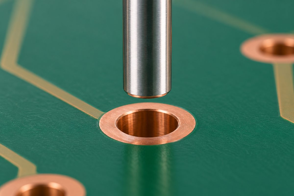
That arithmetic does not prove that the complete assembly will fit. It assumes circular features and ignores positional relationships, shape variation, and other interface conditions. The 0.10 mm diametral difference is not automatically available equally on both sides once the pin and opening are off-center.
Use the component manufacturer’s drawing for the actual mating dimensions and mounting recommendations. For a non-circular lead, review the relevant cross-section rather than using only one width. For a press-fit component, use its specified finished-hole and construction requirements; a loose-clearance example cannot establish the correct interference fit.
If component data and board limits do not establish fit clearly, send the component drawing, proposed finished-hole limits, and board construction for an engineering and quotation review. Identify which features control the interface before changing hole sizes.
Evaluate the complete hole pattern
A multi-pin connector can fail to seat even when each individual hole is large enough. Pin location and hole location must work together across the pattern. Inspect the relationship between features, not only the nominal diameter of one opening.
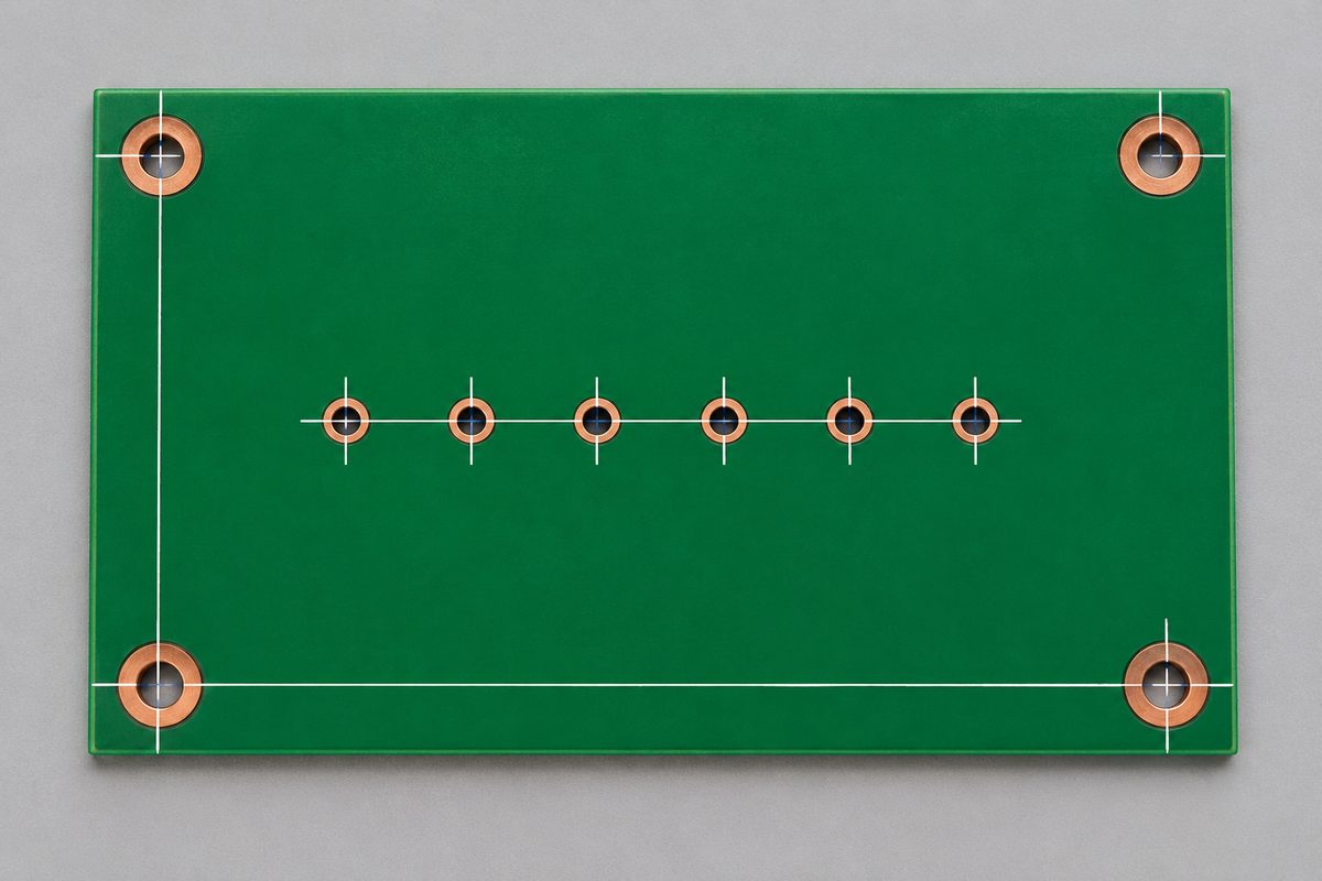
Define the datum or reference system in the mechanical documentation. If the enclosure locates the board from mounting holes, a dimension from an unrelated board edge may not adequately describe the required interface. If an edge controls the fit, confirm how its profile tolerance relates to the holes.
Use consistent definitions for location requirements. Coordinate deviations and a geometric position requirement are not interchangeable merely because they contain the same number. Avoid converting between them informally; the measurement and acceptance approach should follow the governing drawing convention.
Where several tolerances contribute to fit, document the model used for the assessment. Do not simply add every value in a catalog or assume that nominal alignment eliminates accumulated variation. Review the actual interface with the relevant engineering owners.
Specify critical holes locally, not vaguely
A blanket note requesting “tight drill tolerance” is difficult to quote or inspect. Identify the holes that need special control, their nominal sizes and limits, their plating designation, and the location requirements that matter.
Altium’s pad and via documentation describes hole tolerance attributes with minimum and maximum deviations. Such CAD fields can support the design definition, but verify how the chosen output and fabrication drawing communicate them to the recipient. A value present in the editor is not enough if it is absent from the released documentation.
For holes governed by the fabricator’s standard conditions, obtain the applicable conditions for the order rather than assuming an internet value. For critical holes, ask for explicit confirmation of the requested limits. Keep special requirements distinguishable from ordinary via data.
Use the PCB manufacturing capabilities page as a starting point, then confirm the required combination of hole type, size, board construction, and inspection. No general capability listing approves a particular connector fit by itself.
Check design changes for secondary effects
Making a hole larger can improve insertion clearance, but it may reduce the copper margin or clearance to nearby features. Increasing the surrounding land to compensate may consume routing space or conflict with adjacent pads. Recheck the relevant copper layers after either change.
Making a hole smaller can improve nominal copper margin while preventing a lead from entering. Do not shrink a component hole simply to clear a design-rule warning. Resolve the competing requirements explicitly, using the component drawing and confirmed fabrication rules.
A tighter tolerance may change the supplier’s review, inspection, or process plan. It should be justified by a functional need, not imposed globally because tighter sounds better. Ask how the requirement affects the actual quotation and agreed acceptance evidence rather than asserting a fixed cost or lead-time penalty.
When requirements compete, request a review with the critical-hole list, mating drawings, and acceptable design alternatives. This gives the supplier a specific problem to assess instead of an unexplained demand for maximum precision everywhere.
Keep the fabrication files and drawings aligned
Match the drill file, copper, profile, stackup, and hole requirement table to the same released board revision. If a late connector change modifies only a few holes, regenerate and inspect the complete affected package so old dimensions do not remain in a companion drawing.
Our Excellon drill-file release guide explains units, coordinate interpretation, and tool-table checks. Those exchange checks prevent a file interpretation problem from being mistaken for manufacturing variation.
Distinguish nominal coordinate precision from production tolerance. An export that writes many decimal places does not establish that the finished board is held to that resolution. The agreed drawing and order requirements define acceptance; numerical formatting defines how the design data is communicated.
Agree on inspection evidence before ordering
Diameter and position require different evidence. A gauge or dimensional result concerning opening size does not automatically establish the hole’s location relative to a datum. An assembly fit check is useful for its intended purpose but may not document all drawing requirements.
Eurocircuits’ final-inspection overview treats finished diameter and hole position as separate checks. Its equipment and sampling practice illustrate the distinction; they are not an AssyPCB inspection promise.
For critical features, agree on what will be measured, the applicable requirement, the sample or coverage plan, and how results will be tied to the board revision. Preserve actual results rather than recording only a generic pass label without the inspected feature or basis.
Release checklist
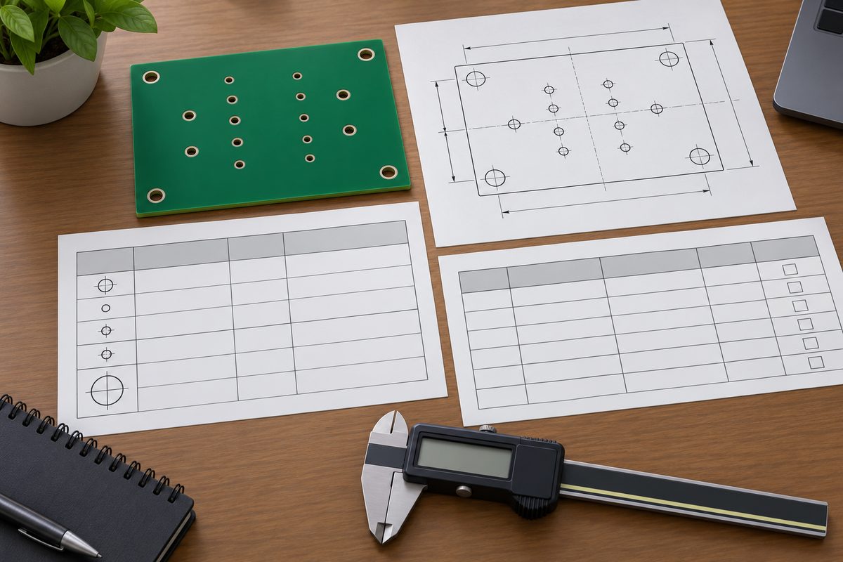
- Identify plated status and the function of each critical hole.
- State finished-size limits in explicit units.
- Define location references separately from size limits.
- Check mating geometry and the full hole pattern.
- Review copper margins and spacing after changes.
- Confirm export interpretation and consistent file revisions.
- Agree on inspection evidence tied to the drawing requirements.
Before placing the order, submit the final fabrication package, quantities, critical-hole table, and required inspection evidence for review and quotation. Separating size, position, and copper registration makes the requirement easier to manufacture, inspect, and approve without relying on an undefined “drill tolerance.”
Latest Blog




Contact Info
Phone: +86-755-82882936
Email: [email protected]
WhatsApp: +86-13570802455
Wechat: +86-13570802455
Address: 2nd floor,D Bldg.,Electric Link Technology Bldg.,Gongming,Guangming New Dist.,518106 Shenzhen, China