
PCB Bow and Twist: Measurement, Assembly Fit, and Supplier Review
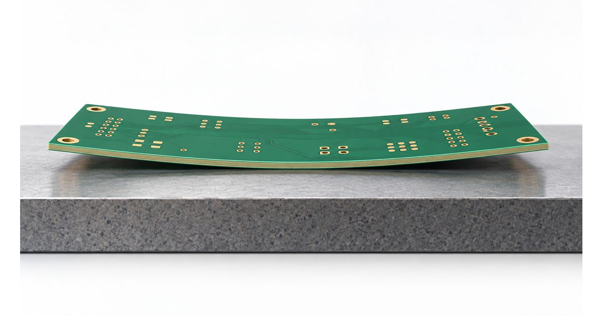
Table of Conent
Table of Conent
PCB bow and twist become purchasing problems when a board that looks acceptable on a desk will not print consistently, travel reliably through assembly equipment, or fit its enclosure without being forced. The useful question is not simply whether a board is curved. It is whether the delivered board meets the agreed flatness requirement under a defined measurement method, and whether that requirement supports the intended assembly process.
A practical review connects three records: the fabrication drawing, the flatness measurement, and the assembly constraints. This guide explains how to bring those records together without treating a photograph as a measurement, a common industry percentage as a universal acceptance limit, or a flattening operation as an automatic repair.
Separate bow, twist, and the condition being inspected
Bow describes broad curvature; for a rectangular board, the corners remain coplanar. Twist describes diagonal distortion that puts a corner outside the plane established by the other three. A board may show a combination rather than one clean shape. The distinction matters because measurement arrangements and calculations differ.
IPC-TM-650 Method 2.4.22C covers rigid boards, rigid portions of rigid-flex boards, and panels. It distinguishes production checks from a referee method and explicitly excludes the special considerations needed for populated assemblies. Identify the specimen and applicable procedure before interpreting any reported percentage.
Keep the following inspection conditions separate in the order documents:
- Individual bare board: the finished circuit after separation, if that is the specified delivery form.
- Delivered assembly panel: the circuits, rails, and remaining connections as supplied to assembly.
- Populated assembly: a different mechanical system, with components, connectors, and supports.
- After a defined thermal exposure: a specified evaluation condition, not interchangeable with an incoming room-temperature check.
Record whether the board was inspected before or after depanelization. A panel result alone should not be labeled an individual-board result. Likewise, a post-assembly observation should not silently replace the incoming inspection record.
Measure with a method, not with a photograph
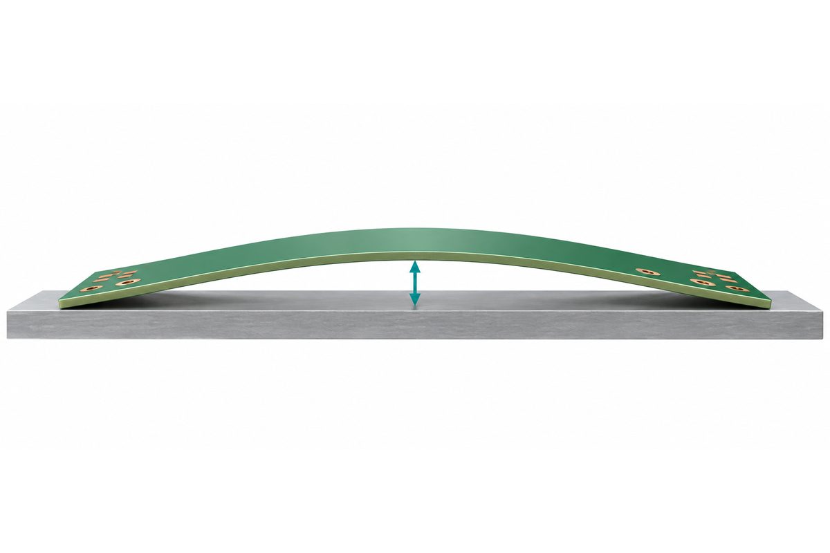
A photograph can document orientation and help explain a complaint, but perspective and uncontrolled support make it insufficient for a numerical flatness decision. Ask for the applicable procedure, board dimensions, datum arrangement, instrument identification, and the observations used to calculate the result.
The cited IPC method uses different dimensional references for bow and twist. Its production twist calculation includes a factor related to the specified corner restraint; that calculation must not be transferred to a different support arrangement. When the production arrangement is unsuitable, the method provides a referee approach. Nonrectangular outlines require special evaluation rather than unquestioned use of rectangular assumptions.
For a supplier report, request both the measured dimensional quantities and the resulting percentage. This makes an incorrect dimension, unit conversion, or calculation easier to identify. A report containing only “warpage passed” cannot show whether the agreed requirement was actually evaluated.
Do not press the board flat to make a convenient reading unless that restraint belongs to the selected procedure. Describe the orientation and any restraint explicitly. If two parties obtain different results, first reproduce the same setup and specimen condition before concluding that either instrument or supplier is wrong.
Write an acceptance requirement that matches the application
A test method explains how to measure; the purchase requirement defines what is acceptable. Specify the applicable acceptance document and edition, any relevant product requirements, and the agreed limit. Do not assume that an internet summary supplies the controlling contractual requirement for every board.
Assembly fit may require a separate discussion even when a bare board meets its fabrication requirement. Eurocircuits’ flatness guidance describes implications for paste application, equipment transport, component mounting, and enclosure installation. Use those concerns to ask application-specific questions rather than to promise a particular process yield.
Tell the fabricator which condition will control incoming acceptance and tell the assembler where support is available. A long unsupported region, a connector alignment requirement, or a mechanically constrained enclosure deserves review before ordering. The drawing should not leave the supplier guessing whether acceptance concerns a delivered panel, a separated circuit, or an assembled product.
For a new project, send the board outline, delivery form, and flatness requirement for a fabrication quote review. Include the assembly constraints alongside the electrical files so the requirement can be discussed before release.
Review construction without compromising electrical design
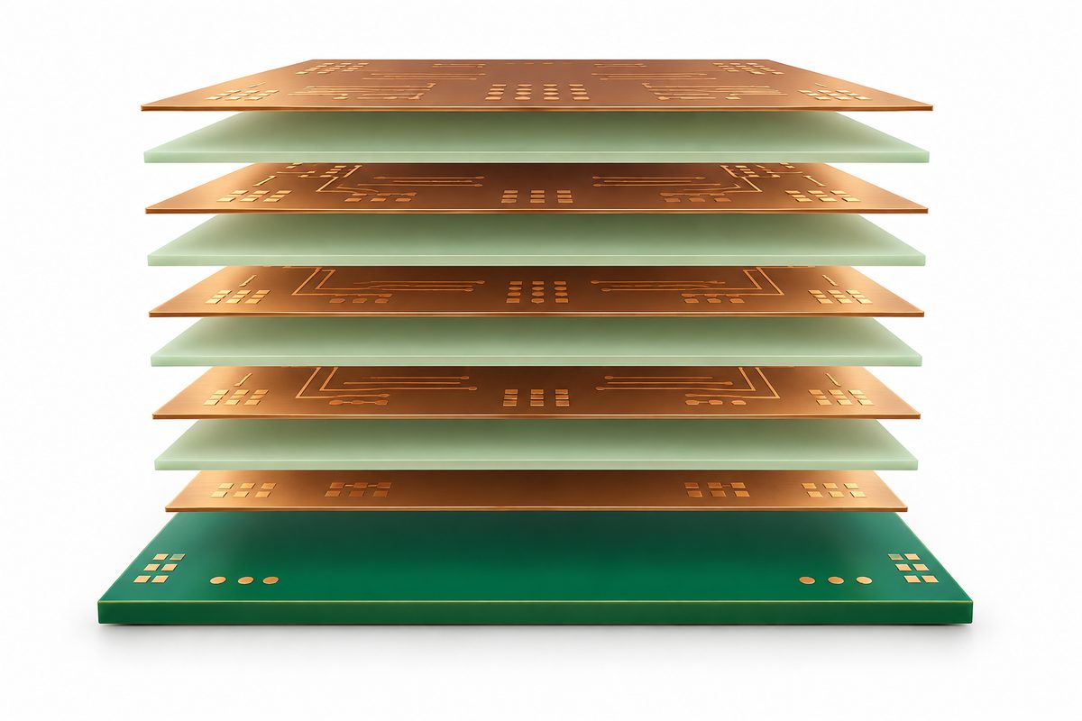
Construction symmetry and copper distribution are useful review topics, not guarantees of flatness. Uneven copper coverage and asymmetric construction can contribute to deformation through manufacturing thermal cycles. Compare the approved stackup with the actual artwork instead of considering total layer count alone.
The Eurocircuits panel copper-distribution guidance identifies balanced copper as a contributor to mechanical stability. For a design review, examine the circuits and the surrounding panel area together. Additional copper or revised panel features should be agreed changes, not unrecorded supplier edits.
Do not add copper solely to make a visual heat map look balanced. Review isolation, creepage, controlled impedance, return paths, antenna keepouts, and test access before changing artwork. If the design cannot be symmetrical, document the reason and ask the supplier to assess that specific construction.
Our PCB lamination guide provides context for stackup and fabrication discussions. Bring the final layer materials and permitted substitutions into the review; a drawing note that names only a generic board material leaves important construction details unresolved.
Connect flatness to thickness, handling, and assembly support
Review board thickness as part of the mechanical design, not as a universal cure for curvature. A thickness change can affect connector engagement, enclosure clearances, mounting hardware, and the electrical stackup. Compare these interfaces before accepting a proposal to make the board thicker.
The PCB thickness selection guide explains how finished tolerances and mechanical fit belong in the same discussion. For a flatness-sensitive assembly, add the unsupported spans and support locations to that information.
Ask the assembler to identify the stage where the problem appears: incoming loading, printing, placement, thermal processing, depanelization, or final installation. Keep these observations separate from the bare-board acceptance decision. Fixture support may help a particular operation, but it does not automatically demonstrate compliance with a delivered-board requirement.
Avoid informal baking schedules, pressing boards under weights, or bending them by hand as default corrective actions. Any proposed conditioning or straightening needs an approved process, product-specific assessment, traceability, and reinspection. A board that temporarily lies flat is not by itself evidence that the underlying issue has been resolved.
Build a supplier report that supports a decision
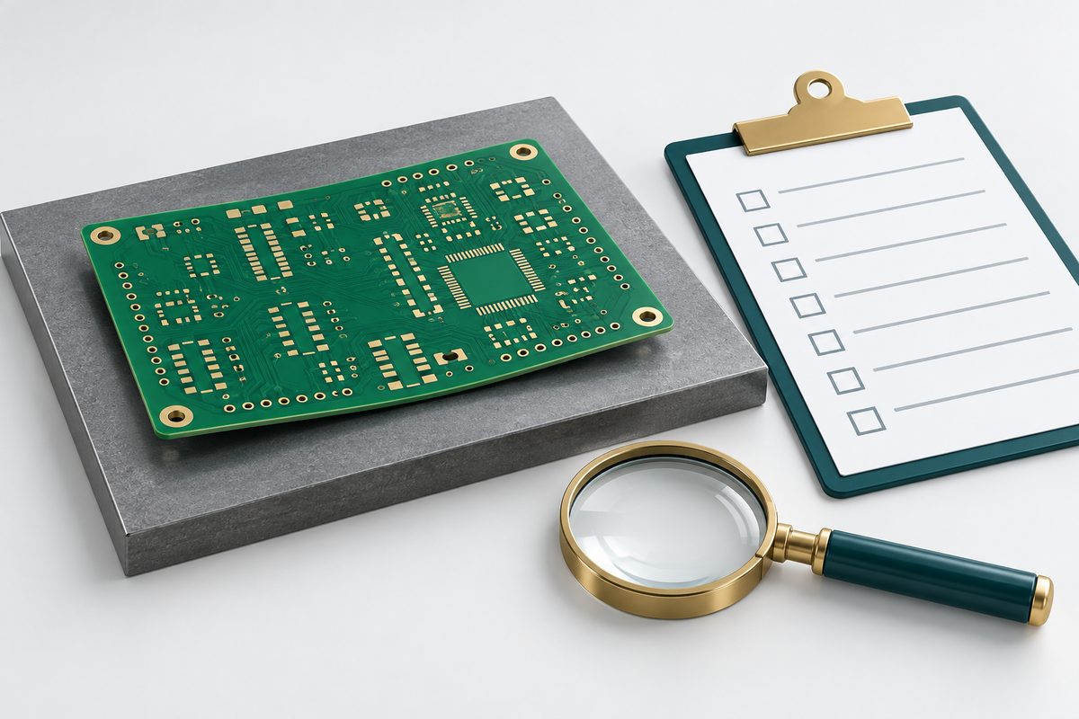
A usable report links each result to a traceable sample. Request board number and revision, lot identity, delivery condition, sample selection, measurement date, method and revision, equipment, raw observations, calculated result, and acceptance basis. Include photographs as supporting records with the board orientation identified.
Preserve individual results rather than accepting only a lot average. The agreed sampling plan should explain how inspected pieces represent the shipment and how exceptions are handled. Do not infer that an entire lot complies because one convenient sample does.
If incoming and supplier results disagree, compare the same specimens where practical. Check whether dimensions refer to the same delivery form and whether either party changed support, restraint, or conditioning. Record unresolved differences instead of averaging incompatible measurements into a reassuring number.
Request a manufacturing review with your flatness report and controlled drawing when you need the construction, measurement condition, and acceptance requirement discussed together. Specify the evidence expected with the order rather than assuming every report format is included.
A hypothetical panel-to-board review
Consider a buyer who receives a panel report but finds that separated boards do not sit consistently in an assembly nest. No percentage is assumed in this example, and it is not an AssyPCB production case.
The buyer first checks whether acceptance was defined for panels or individual circuits. Next, the teams document the separation process and compare identified samples before and after separation. They review the nest’s support locations separately, then decide which measurement condition belongs in the revised purchase drawing. This avoids rejecting a shipment against an unstated requirement or changing the assembly fixture without investigating the board condition.
Prepare the next RFQ around evidence
Include the controlled artwork, stackup, finished thickness tolerance, panel drawing, delivery form, flatness acceptance basis, and assembly constraints. State which design changes are permitted and which require approval. Ask the supplier to identify any additional evaluation needed for an unusual outline or populated assembly.
Use the published PCB manufacturing capabilities as a starting point, then confirm the requested construction and inspection scope for your project. Do not treat a general capability page as confirmation of a custom flatness limit or special qualification.
Submit your PCB files and assembly-fit requirements for a project-specific quote. A clear requirement and a reproducible report provide a stronger basis for purchasing than a visual judgment that the board looks flat enough.
Latest Blog
Contact Info
Phone: +86-755-82882936
Email: [email protected]
WhatsApp: +86-13570802455
Wechat: +86-13570802455
Address: 2nd floor,D Bldg.,Electric Link Technology Bldg.,Gongming,Guangming New Dist.,518106 Shenzhen, China